AD9516-4/PCBZ Analog Devices Inc, AD9516-4/PCBZ Datasheet - Page 78
AD9516-4/PCBZ
Manufacturer Part Number
AD9516-4/PCBZ
Description
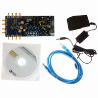
BOARD EVAL FOR AD9516-4 1.8GHZ
Manufacturer
Analog Devices Inc
Specifications of AD9516-4/PCBZ
Main Purpose
Timing, Clock Generator
Embedded
No
Utilized Ic / Part
AD9516-4
Primary Attributes
2 Inputs, 14 Outputs, 1.6GHz VCO
Secondary Attributes
CMOS, LVDS, LVPECL Output Logic, ADIsimCLK™ Graphical User Interface
Silicon Manufacturer
Analog Devices
Application Sub Type
PLL Clock Synthesizer
Kit Application Type
Clock & Timing
Silicon Core Number
AD9516-0, AD9516-1, AD9516-2
Silicon Family Name
AD9516-X
Rohs Compliant
Yes
Lead Free Status / RoHS Status
Lead free / RoHS Compliant


AD9516-4
LVPECL CLOCK DISTRIBUTION
The LVPECL outputs of the AD9516 provide the lowest jitter
clock signals that are available from the AD9516. The LVPECL
outputs (because they are open emitter) require a dc termination
to bias the output transistors. The simplified equivalent circuit
in Figure 59 shows the LVPECL output stage.
In most applications, an LVPECL far-end Thevenin termination
(see Figure 71) or Y-termination (see Figure 72) is recommended.
In each case, the V
VS_LVPECL. If it does not, ac coupling is recommended (see
Figure 73).
The resistor network is designed to match the transmission line
impedance (50 Ω) and the switching threshold (V
VS_LVPECL
Figure 71. DC-Coupled 3.3 V LVPECL, Far-End Thevenin Termination
VS_LVPECL
VS_LVPECL
LVPECL
Figure 73. AC-Coupled LVPECL with Parallel Transmission Line
LVPECL
LVPECL
200Ω
Figure 72. DC-Coupled 3.3 V LVPECL, Y-Termination
0.1nF
0.1nF
S
(NOT COUPLED)
200Ω
SINGLE-ENDED
of the receiving buffer should match the
Z
Z
0
0
TRANSMISSION LINE
100Ω DIFFERENTIAL
50Ω
50Ω
= 50Ω
= 50Ω
(COUPLED)
127Ω
83Ω
VS_DRV
50Ω
100Ω
50Ω
50Ω
127Ω
83Ω
V
S
LVPECL
LVPECL
V
= 3.3V
S
S
− 1.3 V).
LVPECL
V
S
Rev. A | Page 78 of 80
LVPECL Y-termination is an elegant termination scheme that
uses the fewest components and offers both odd- and even-mode
impedance matching. Even-mode impedance matching is an
important consideration for closely coupled transmission lines
at high frequencies. Its main drawback is that it offers limited
flexibility for varying the drive strength of the emitter-follower
LVPECL driver. This can be an important consideration when
driving long trace lengths but is usually not an issue. In the case
shown in Figure 72, where VS_LVPECL = 2.5 V, the 50 Ω
termination resistor that is connected to ground should be
changed to 19 Ω.
Thevenin-equivalent termination uses a resistor network to provide
50 Ω termination to a dc voltage that is below V
driver. In this case, VS_LVPECL on the AD9516 should equal V
of the receiving buffer. Although the resistor combination shown
in Figure 72 results in a dc bias point of VS_LVPECL − 2 V, the
actual common-mode voltage is VS_LVPECL − 1.3 V because
additional current flows from the AD9516 LVPECL driver through
the pull-down resistor.
The circuit is identical when VS_LVPECL = 2.5 V, except that
the pull-down resistor is 62.5 Ω and the pull-up resistor is 250 Ω.
LVDS CLOCK DISTRIBUTION
The AD9516 provides four clock outputs (OUT6 to OUT9) that
are selectable as either CMOS or LVDS level outputs. LVDS is a
differential output option that uses a current mode output stage.
The nominal current is 3.5 mA, which yields 350 mV output swing
across a 100 Ω resistor. An output current of 7 mA is also available
in cases where a larger output swing is required. The LVDS
output meets or exceeds all ANSI/TIA/EIA-644 specifications.
A recommended termination circuit for the LVDS outputs is
shown in Figure 74.
See the
Speed Analog-to-Digital Converters for more information on LVDS.
AN-586 Application
VS
LVDS
Figure 74. LVDS Output Termination
DIFFERENTIAL (COUPLED)
100Ω
Note, LVDS Data Outputs for High-
100Ω
OL
VS
LVDS
of the LVPECL
S
Related parts for AD9516-4/PCBZ
Image
Part Number
Description
Manufacturer
Datasheet
Request
R

Part Number:
Description:
IC CLOCK PLL/VCO 2GHZ 64LFCSP
Manufacturer:
Analog Devices Inc
Datasheet:
Part Number:
Description:
IC CLOCK GEN 2.8GHZ VCO 64-LFCSP
Manufacturer:
Analog Devices Inc
Datasheet:
Part Number:
Description:
IC,Fourteen Distributed-Output Clock Driver,LLCC,64PIN,PLASTIC
Manufacturer:
Analog Devices Inc
Datasheet:
Part Number:
Description:
IC,Ten Distributed-Output Clock Driver,LLCC,64PIN,PLASTIC
Manufacturer:
Analog Devices Inc
Datasheet:
Part Number:
Description:
IC,Ten Distributed-Output Clock Driver,LLCC,64PIN,PLASTIC
Manufacturer:
Analog Devices Inc
Datasheet:
Part Number:
Description:
Clock IC With 1.8GHz On-chip VCO
Manufacturer:
Analog Devices Inc
Datasheet:

Part Number:
Description:
BOARD EVAL FOR AD9516-2 2.2GHZ
Manufacturer:
Analog Devices Inc
Datasheet:

Part Number:
Description:
Clock IC With 2.5GHz On-chip VCO EB
Manufacturer:
Analog Devices Inc
Datasheet:
Part Number:
Description:
IC CLOCK GEN 2.8GHZ VCO 64-LFCSP
Manufacturer:
Analog Devices Inc
Datasheet:
Part Number:
Description:
IC,Ten Distributed-Output Clock Driver,LLCC,64PIN,PLASTIC
Manufacturer:
Analog Devices Inc
Datasheet:
Part Number:
Description:
IC,Fourteen Distributed-Output Clock Driver,LLCC,64PIN,PLASTIC
Manufacturer:
Analog Devices Inc
Datasheet:
Part Number:
Description:
IC,Ten Distributed-Output Clock Driver,LLCC,64PIN,PLASTIC
Manufacturer:
Analog Devices Inc
Datasheet:
Part Number:
Description:
Clock IC With 1.8GHz On-chip VCO
Manufacturer:
Analog Devices Inc
Datasheet:
Part Number:
Description:
10/14 Chan Clock IC W/PLL-no VCO
Manufacturer:
Analog Devices Inc
Datasheet:
Part Number:
Description:
10/14 Chan Clock IC W/PLL-no VCO
Manufacturer:
Analog Devices Inc
Datasheet: