AD9954/PCBZ Analog Devices Inc, AD9954/PCBZ Datasheet - Page 20
AD9954/PCBZ
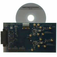
Manufacturer Part Number
AD9954/PCBZ
Description
BOARD EVAL FOR 9954
Manufacturer
Analog Devices Inc
Series
AgileRF™r
Datasheet
1.AD9954YSVZ-REEL7.pdf
(40 pages)
Specifications of AD9954/PCBZ
Main Purpose
Timing, Direct Digital Synthesis (DDS)
Embedded
No
Utilized Ic / Part
AD9954
Primary Attributes
14-Bit DAC, 32-Bit Tuning Word Width
Secondary Attributes
400MHz, Graphical User Interface
Lead Free Status / RoHS Status
Lead free / RoHS Compliant


AD9954
The last method in which the sweep ramp rate timer can be
reset is changing from inactive linear sweep mode to active
linear sweep mode using the linear sweep enable bit (CFR1<21>).
For methods two and three, the ramp rate timer loads a value
determined by the state of PS0 (0 = FSRRW, 1 = RSRRW).
Power-Down Functions of the AD9954
The AD9954 supports an externally controlled (or hardware)
power-down feature as well as software-programmable power-
down bits capable of individually powering down specific unused
circuit blocks.
Table 9. Power-Down Control Functions
Control
PWRDWNCTL = 0, CFR1<3> don’t care
PWRDWNCTL = 1, CFR1<3> = 0
PWRDWNCTL = 1, CFR1<3> = 1
Mode Active
Software control
External control, fast recovery
power-down mode
External control, full power-down
mode
Rev. B | Page 20 of 40
Software-controlled power-down enables individual powering
down of the DAC, comparator, PLL, input clock circuitry, and
the digital logic (CFR1<7:4>). With the exception of CFR1<6>,
these bits are superseded when the externally controlled power-
down pin (PWRDWNCTL) is high. External power-down
control is supported on the AD9954 via the PWRDWNCTL
input pin. When the PWRDWNCTL input pin is high, the
AD9954 enters a power-down mode based on the CFR1<3> bit.
When the PWRDWNCTL input pin is low, it operates normally.
See CFR1<3> in Table 12 for details.
Table 9 details the logic level for each power-down bit that
drives out of the AD9954 core logic to the analog section and
the digital clock generation section of the chip for the external
power-down operation.
Description
Digital power-down = CFR1<7>
Comparator power-down = CFR1<6>
DAC power-down = CFR1<5>
Clock input power-down = CFR1<4>
Digital power-down = 1’b1
Comparator power-down = 1’b0 or CFR1<6>
DAC power-down = 1’b0
Clock input power-down = 1’b0
Digital power-down = 1’b1
Comparator power-down = 1’b1
DAC power-down = 1’b1
Clock input power-down = 1’b1
Related parts for AD9954/PCBZ
Image
Part Number
Description
Manufacturer
Datasheet
Request
R

Part Number:
Description:
BOARD EVAL FOR AD9954
Manufacturer:
Analog Devices Inc
Datasheet:


Part Number:
Description:
±1.7g Dual-Axis IMEMS Accelerometer Evaluation Board
Manufacturer:
Analog Devices Inc
Datasheet:
Part Number:
Description:
Inertial Sensor Evaluation System
Manufacturer:
Analog Devices Inc
Datasheet:
Part Number:
Description:
Manufacturer:
Analog Devices Inc
Datasheet:
Part Number:
Description:
Manufacturer:
Analog Devices Inc
Datasheet:
Part Number:
Description:
Manufacturer:
Analog Devices Inc
Datasheet:
Part Number:
Description:
Manufacturer:
Analog Devices Inc
Datasheet:
Part Number:
Description:
Manufacturer:
Analog Devices Inc
Datasheet:
Part Number:
Description:
Manufacturer:
Analog Devices Inc
Datasheet:
Part Number:
Description:
Manufacturer:
Analog Devices Inc
Datasheet:
Part Number:
Description:
Manufacturer:
Analog Devices Inc
Datasheet:
Part Number:
Description:
Manufacturer:
Analog Devices Inc
Datasheet: