STEVAL-IPT002V1 STMicroelectronics, STEVAL-IPT002V1 Datasheet - Page 18
STEVAL-IPT002V1
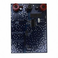
Manufacturer Part Number
STEVAL-IPT002V1
Description
BOARD EVAL SMART CARD
Manufacturer
STMicroelectronics
Specifications of STEVAL-IPT002V1
Main Purpose
Memory, Smart Card
Embedded
No
Utilized Ic / Part
ST8024
Primary Attributes
New Digital Systems (NDS) Compatible
Secondary Attributes
Short-Circuit & Thermal Protection
Product
Power Management Modules
Silicon Manufacturer
ST Micro
Silicon Core Number
ST8024
Kit Application Type
Interface
Application Sub Type
Smart Card Interface
Kit Contents
Board CD Docs
Lead Free Status / RoHS Status
Lead free / RoHS Compliant
Other names
497-8939
Available stocks
Company
Part Number
Manufacturer
Quantity
Price
Company:

Part Number:
STEVAL-IPT002V1
Manufacturer:
STMicroelectronics
Quantity:
1


5.4
18/31
Table 21.
1. The status of pins CLKDIV1 and CLKDIV2 must not be changed simultaneously; a delay of 10 ns minimum
The frequency change is synchronous, which means that during transition no pulse is
shorter than 45 % of the smallest period, and that the first and last clock pulses about the
instant of change have the correct width.
When changing the frequency dynamically, the change is effective for only eight periods of
XTAL1 after the command. The duty factor of f
XTAL1. In order to reach a 45 to 55 % duty factor on pin CLK, the input signal on pin XTAL1
should have a duty factor of 48 to 52 % and transition times of less than 5 % of the input
signal period.
If a crystal is used, the duty factor on pin CLK may be 45 to 55 % depending on the circuit
layout and on the crystal characteristics and frequency. In other cases, the duty factor on pin
CLK is guaranteed between 45 and 55 % of the clock period.
The crystal oscillator runs as soon as the IC is powered up. If the crystal oscillator is used,
or if the clock pulse on pin XTAL1 is permanent, the clock pulse is applied to the card as
shown in the activation sequences shown in
If the signal applied to XTAL1 is controlled by the system microcontroller, the clock pulse will
be applied to the card when it is sent by the system microcontroller (after completion of the
activation sequence).
I/O transceivers
The three data lines I/O, AUX1 and AUX2 are identical.The idle state is realized by both I/O
and I/OUC lines being pulled HIGH via a 11 kΩ resistor (I/O to V
I/O is referenced to V
equal to V
An anti-latch circuit disables the detection of falling edges on the line of the other side, which
then becomes a slave. After a time delay t
on, thus transmitting the logic 0 present on the master side. When the master side returns to
logic 1, a P transistor on the slave side is turned on during the time delay t
sides return to their idle states. This active pull-up feature ensures fast LOW-to-HIGH
transitions; it is able to deliver more than 1 mA at an output voltage of up to 0.9 V
80 pF load. At the end of the active pull-up pulse, the output voltage depends only on the
internal pull-up resistor and the load current. The current to and from the card I/O lines is
limited internally to 15 mA and the maximum frequency on these lines is 1 MHz.
between changes is needed; the minimum duration of any state of CLK is eight periods of XTAL1.
DD
CLKDIV1
. The first side of the transceiver to receive a falling edge becomes the master.
Clock frequency selection
0
0
1
1
CC
, and pin I/OUC to V
(1)
CLKDIV2
d(edge)
DD
Figure 5
0
1
1
0
XTAL
, thus allowing operation when V
, an N transistor on the slave side is turned
depends on the signal present at pin
and
Figure 6
CC
and I/OUC to V
f
f
f
XTAL
XTAL
XTAL
f
pu
f
XTAL
CLK
and then both
/8
/4
/2
CC
CC
is not
DD
into an
). Pin
Related parts for STEVAL-IPT002V1
Image
Part Number
Description
Manufacturer
Datasheet
Request
R

Part Number:
Description:
BOARD DEMO TFT DISPLAY STR91
Manufacturer:
STMicroelectronics
Datasheet:

Part Number:
Description:
BOARD EVAL FOR MEMS SENSORS
Manufacturer:
STMicroelectronics
Datasheet:

Part Number:
Description:
KIT DEV STARTER ST10F276Z5
Manufacturer:
STMicroelectronics
Datasheet:

Part Number:
Description:
BOARD EVAL HDMI $ VIDEO SWITCH
Manufacturer:
STMicroelectronics
Datasheet:

Part Number:
Description:
BOARD DEMO ACCELEROMETER DIL24
Manufacturer:
STMicroelectronics
Datasheet:

Part Number:
Description:
BOARD STLM75/STDS75/ST72F651
Manufacturer:
STMicroelectronics
Datasheet:

Part Number:
Description:
EVAL BOARD 3AXIS MEMS ACCELLRMTR
Manufacturer:
STMicroelectronics
Datasheet:

Part Number:
Description:
BOARD EVAL 8BIT MICRO + TDE1708
Manufacturer:
STMicroelectronics
Datasheet:

Part Number:
Description:
EVAL BOARD A/D TS4657
Manufacturer:
STMicroelectronics
Datasheet:

Part Number:
Description:
BOARD ADAPTER 20DIP LIS3LV02DL
Manufacturer:
STMicroelectronics
Datasheet:
Part Number:
Description:
STMicroelectronics [RIPPLE-CARRY BINARY COUNTER/DIVIDERS]
Manufacturer:
STMicroelectronics
Datasheet:
Part Number:
Description:
STMicroelectronics [LIQUID-CRYSTAL DISPLAY DRIVERS]
Manufacturer:
STMicroelectronics
Datasheet:
Part Number:
Description:
BOARD EVAL FOR MEMS SENSORS
Manufacturer:
STMicroelectronics
Datasheet: