STEVAL-CCH002V1 STMicroelectronics, STEVAL-CCH002V1 Datasheet - Page 14
STEVAL-CCH002V1
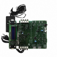
Manufacturer Part Number
STEVAL-CCH002V1
Description
BOARD EVAL HDMI $ VIDEO SWITCH
Manufacturer
STMicroelectronics
Specifications of STEVAL-CCH002V1
Design Resources
STEVAL-CCH002V1 Gerber Files STEVAL-CCH002V1 Schematic STEVAL-CCH002V1 Bill of Material
Main Purpose
Video, HDMI and Video Switches
Embedded
Yes, MCU, 8-Bit
Utilized Ic / Part
STMAV335, STMAV340, STHDMI002A, STDVE003A
Primary Attributes
DVI-I, 2 HDMI, Y Pb Pr, S-Video, CVBS, VGA - Input and Output
Secondary Attributes
LCD Displays Selection Status of Video Switches and Buffers
Lead Free Status / RoHS Status
Lead free / RoHS Compliant
Other names
497-8371


Functional description
3.5
3.6
3.7
14/42
I
The device contains two identical bidirectional open-drain, non-inverting buffer circuits that
enable I
STDVE003A buffers both the serial data (DDC SDA) and serial clock (DDC SCL) on the I2C
bus, while retaining all the operating modes and features of the I
two buses of 400 pF bus capacitance to be connected in an I
are operational from a supply V of 3.0 V to 3.6 V.
The I
STDVE003A enables the system designer to isolate the two halves of a bus,
accommodating more I
buses, one at 5 V and the other at 3.3 V or a 400 kHz and 100 kHz bus, where the 100 kHz
bus is isolated when 400 kHz operation of the other bus is required. The STDVE003A can
be used to run the I
The S1, S2 and S3 (SEL) lines act as control signals for the corresponding A, B or C ports.
Note that the SEL line has an internal pull-down resistor. The SEL line should not change
state during an I
enabling part way through a bus cycle could confuse the I
input should change state only when the global bus and the repeater port are in idle state, to
prevent system failures.
The output low levels for each internal buffer are approximately 0.5 V, but the input voltage
of each internal buffer must be 70 mV or more below the output low level, when the output
internally is driven low. This prevents a lock-up condition from occurring when the input low
condition is released.
As with the standard I
levels on the buffered bus. The STDVE003A has standard open collector configuration of
the I
repeater must have a pull up resistor.
This part is designed to work with standard mode and fast mode I
mode I
in a generic I
Under certain conditions, higher termination currents can be used.
Power-down condition
The OE_N is used to disable most of the internal circuitry of STDVE003A that puts the
device in a low power mode of operation.
Bias
The bandgap reference voltage over the external R
bias reference current. This current and its factors (achieved by employing highly accurate
and well matched current mirror circuit topologies) are generated on-chip and used by
several internal modules. The 10 mA current used by the transmitter block is also generated
using this reference current. It is important to ensure that the R
tolerance range of its typical value.
2
C DDC line repeater
2
2
C bus. The size of the pull up resistors depends on the system, but each side of the
C bus capacitance limit of 400 pF restricts the number of devices and bus length. The
2
C devices only specify 3 mA output drive, this limits the termination current to 3 mA
2
C DDC bus lines to be extended without degradation in system performance. The
2
C system where standard mode devices and multiple masters are possible.
2
C operation, because disabling during bus operation hangs the bus and
2
C bus at both 5 V and 3.3 V interface levels.
2
C system, pull up resistors are required to provide the logic high
2
C devices or longer trace lengths. It can also be used to run two
EXT
reference resistor sets the internal
2
C parts being enabled. The SEL
2
C application. These buffers
EXT
2
C system. This enables
2
C devices. Standard
value is within the ±1%
STDVE003A
Related parts for STEVAL-CCH002V1
Image
Part Number
Description
Manufacturer
Datasheet
Request
R

Part Number:
Description:
EVAL BOARD CC DRVR HI DENSE LEDS
Manufacturer:
STMicroelectronics
Datasheet:

Part Number:
Description:
EVAL BOARD CC DRVR HI DENSE LEDS
Manufacturer:
STMicroelectronics
Datasheet:

Part Number:
Description:
BATTERY CHARGER CELL PHONE
Manufacturer:
STMicroelectronics
Datasheet:

Part Number:
Description:
BOARD EVAL FOR MEMS SENSORS
Manufacturer:
STMicroelectronics
Datasheet:

Part Number:
Description:
KIT DEV STARTER ST10F276Z5
Manufacturer:
STMicroelectronics
Datasheet:

Part Number:
Description:
BOARD EVAL UPS 450W VOUT=220V
Manufacturer:
STMicroelectronics
Datasheet:

Part Number:
Description:
BOARD STLM75/STDS75/ST72F651
Manufacturer:
STMicroelectronics
Datasheet:

Part Number:
Description:
EVAL BOARD ENERGY METER MONO
Manufacturer:
STMicroelectronics
Datasheet:

Part Number:
Description:
EVAL BOARD ENERGY METER MONO
Manufacturer:
STMicroelectronics
Datasheet:

Part Number:
Description:
EVAL BOARD ENERGY METER MONO
Manufacturer:
STMicroelectronics
Datasheet:

Part Number:
Description:
STMicroelectronics [RIPPLE-CARRY BINARY COUNTER/DIVIDERS]
Manufacturer:
STMicroelectronics
Datasheet:
Part Number:
Description:
STMicroelectronics [LIQUID-CRYSTAL DISPLAY DRIVERS]
Manufacturer:
STMicroelectronics
Datasheet:
Part Number:
Description:
BOARD EVAL FOR MEMS SENSORS
Manufacturer:
STMicroelectronics
Datasheet: