DC-VIDEO-TVP5146N Altera, DC-VIDEO-TVP5146N Datasheet - Page 15
DC-VIDEO-TVP5146N
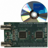
Manufacturer Part Number
DC-VIDEO-TVP5146N
Description
VIDEO DAUGHTER CARD
Manufacturer
Altera
Series
Stratix® IIIr
Datasheets
1.EP3SL150F780C4N.pdf
(16 pages)
2.EP3SL150F780C4N.pdf
(332 pages)
3.DC-VIDEO-TVP5146N.pdf
(58 pages)
Specifications of DC-VIDEO-TVP5146N
Main Purpose
Video, Daughter Card
Embedded
No
Utilized Ic / Part
Altera Dev Kits
Primary Attributes
Dual Composite Video Input - NTSC or PAL
Secondary Attributes
10-bit BT.656 Output, Compatible with Expansion Connector, Standard on Most Altera Development Kits
Lead Free Status / RoHS Status
Lead free / RoHS Compliant
Other names
544-1704


Altera Corporation
f
f
<2S60_DevKit_Install_Directory>\Examples\HW\NiosII
\altera_dsp_dev_board_stratix_2s180
\altera_dsp_dev_board_stratix_2s180.sof
3.
$ nios2-flash-programmer --base=0x01000000
--input=<project_name>.flash
--sof=altera_dsp_dev_board_stratix_2s180.sof
--device=1
For more information on programming the flash memory or loading
SOF files into the on-board flash memory, refer to the Nios II Flash
Programmer User Guide.
The Factory Design
When the Stratix II device is programmed with the factory design, LEDs
D5 through D8 behave as a binary counter that counts down to zero. This
is a power-up indication that the board is functional and the device was
successfully programmed with the factory design.
Along with the LED counter, the factory design includes two blocks of IP
generated by the Altera NCO Compiler. One of these oscillators is
running at 10 times the frequency of the other, but both of them have the
same amplitude, covering 13 bits of dynamic range. Two sine waves
generated by these blocks are added together and the output is converted
from a 2's complement representation into unsigned integer format. This
combined sine wave signal with 14-bit dynamic range is sent to a 14-bit
D/A converter.
When the analog output of the D/A converter is connected, via the
included SMA cable, with the analog input of one of the 12-bit A/D
converters, the A/D converter’s digital output is looped back to the
Stratix II device. The design converts this loopback input from 2's
complement format to unsigned integer format. The converted loopback
data is captured by an instance of the SignalTap
design for display and analysis.
For step-by-step instructions on how to use the factory design to test the
functionality of the board, refer to the DSP Development Kit, Stratix II
Professional Edition Getting Started User Guide.
Move a copy of the flash programming SOF file to your project
directory. The flash programming SOF file is in the location:
Run the Nios II Flash Programmer (nios2-flash-programmer) utility:
Stratix II EP2S180 DSP Development Board Reference Manual
Core Version a.b.c variable
Board Components & Interfaces
®
II logic analyzer in the
2–7
Related parts for DC-VIDEO-TVP5146N
Image
Part Number
Description
Manufacturer
Datasheet
Request
R

Part Number:
Description:
CYCLONE II STARTER KIT EP2C20N
Manufacturer:
Altera
Datasheet:


Part Number:
Description:
CPLD, EP610 Family, ECMOS Process, 300 Gates, 16 Macro Cells, 16 Reg., 16 User I/Os, 5V Supply, 35 Speed Grade, 24DIP
Manufacturer:
Altera Corporation
Datasheet:
Part Number:
Description:
CPLD, EP610 Family, ECMOS Process, 300 Gates, 16 Macro Cells, 16 Reg., 16 User I/Os, 5V Supply, 15 Speed Grade, 24DIP
Manufacturer:
Altera Corporation
Datasheet:
Part Number:
Description:
Manufacturer:
Altera Corporation
Datasheet:
Part Number:
Description:
CPLD, EP610 Family, ECMOS Process, 300 Gates, 16 Macro Cells, 16 Reg., 16 User I/Os, 5V Supply, 30 Speed Grade, 24DIP
Manufacturer:
Altera Corporation
Datasheet:
Part Number:
Description:
High-performance, low-power erasable programmable logic devices with 8 macrocells, 10ns
Manufacturer:
Altera Corporation
Datasheet:
Part Number:
Description:
High-performance, low-power erasable programmable logic devices with 8 macrocells, 7ns
Manufacturer:
Altera Corporation
Datasheet:
Part Number:
Description:
Classic EPLD
Manufacturer:
Altera Corporation
Datasheet:
Part Number:
Description:
High-performance, low-power erasable programmable logic devices with 8 macrocells, 10ns
Manufacturer:
Altera Corporation
Datasheet:
Part Number:
Description:
Manufacturer:
Altera Corporation
Datasheet:
Part Number:
Description:
Manufacturer:
Altera Corporation
Datasheet:
Part Number:
Description:
Manufacturer:
Altera Corporation
Datasheet:
Part Number:
Description:
CPLD, EP610 Family, ECMOS Process, 300 Gates, 16 Macro Cells, 16 Reg., 16 User I/Os, 5V Supply, 25 Speed Grade, 24DIP
Manufacturer:
Altera Corporation
Datasheet: