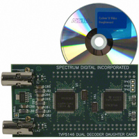
DC-VIDEO-TVP5146N Altera, DC-VIDEO-TVP5146N Datasheet - Page 18

DC-VIDEO-TVP5146N
Manufacturer Part Number
DC-VIDEO-TVP5146N
Description
VIDEO DAUGHTER CARD
Manufacturer
Altera
Series
Stratix® IIIr
Datasheets
1.EP3SL150F780C4N.pdf
(16 pages)
2.EP3SL150F780C4N.pdf
(332 pages)
3.DC-VIDEO-TVP5146N.pdf
(58 pages)
Specifications of DC-VIDEO-TVP5146N
Main Purpose
Video, Daughter Card
Embedded
No
Utilized Ic / Part
Altera Dev Kits
Primary Attributes
Dual Composite Video Input - NTSC or PAL
Secondary Attributes
10-bit BT.656 Output, Compatible with Expansion Connector, Standard on Most Altera Development Kits
Lead Free Status / RoHS Status
Lead free / RoHS Compliant
Other names
544-1704
Functional Description
2–10
Stratix II EP2S180 DSP Development Board Reference Manual
The Stratix II EP2S180 DSP development board can obtain a clock source
from one or more of the following sources:
■
■
The board can provide independent clocks from both the enhanced and
fast PLLs to the A/D converters, the D/A converters, and the other
components that require stable clock sources.
To implement this concept, the enhanced PLL5-dedicated pins drive the
A/D converters and associated functions, and the enhanced
PLL6-dedicated pins drive the D/A converters and associated functions.
Notes to
(1)
(2)
pld_CLKIN0,pld_CLK
IN1
pld_CLKIN0_n,pld_C
LKIN1_n
proto1_OSC,
proto2_OSC
cpld_CLKOSC
adc_CLK_IN1,
adc_CLK_IN2
dac_CLKIN1,
dac_CLKIN2
pld_CLKFB
adc_CLK_IN1_n,
adc_CLK_IN2_n
dac_DACCLKIN1,
dac_DACCLKIN2
pld_DACCLKIN
proto1_CLKOUT,
proto2_CLKOUT
Table 2–4. Clock Distribution Signals (Part 2 of 2)
The on-board crystal oscillator
An external clock (through an SMA connector or a Stratix II pin)
Signal Name
J3 and J4 control which clock is routed to the A/D converters. See
details.
J18 and J19 control which clock is routed to the D/A converters. See
for details.
Table
Core Version a.b.c variable
2–4:
100-MHz oscillator
External CLKIN_n input
(J11)
100-MHz oscillator
100-MHz oscillator
100-MHz oscillator
100-MHz oscillator
pld_CLKOUT signal from
the Stratix II pin J14
External CLKIN_n input
(J11)
External DA_EXT_CLK
input (J12)
External DA_EXT_CLK
input (J12)
PROTO1 (J25 pin 13)
PROTO2 (J28 pin 13) via
a buffer (U7)
Comes From
Stratix II device pins AM17
and A16
Stratix II device pins AL17
and B16
PROTO1 (J25 pin 9) and
PROTO2 (J28 pin 9) via a
buffer (U7)
CPLD (U10 pin 125)
ADC A (U1 pins 8, 7) and B
(U2 pins 8, 7)
DAC A (U14 pin 28) and B
(U15 pin 28)
Stratix II device pin U1
ADC A (U1 pins 8, 7) and B
(U2 pins 8, 7)
DAC A (U14 pin 28) and B
(U15 pin 28)
Stratix II device pin E16
Stratix II device pins T32 and
T30
Altera Corporation
Goes To
(2)
(2)
(1)
(1)
Table 2–10
Table 2–16
for


