NBC124XXEVB ON Semiconductor, NBC124XXEVB Datasheet - Page 11
NBC124XXEVB
Manufacturer Part Number
NBC124XXEVB
Description
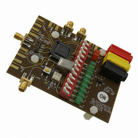
EVAL BOARD FOR NBC124XX
Manufacturer
ON Semiconductor
Datasheets
1.NBC12439FAR2G.pdf
(21 pages)
2.NBC12429FAR2G.pdf
(22 pages)
3.NBC12430FAR2G.pdf
(20 pages)
Specifications of NBC124XXEVB
Design Resources
NBC124XXEVB Gerber Files
Main Purpose
Timing, PLL
Embedded
No
Utilized Ic / Part
NBC12429, NBC12430, NBC12439
Primary Attributes
DIP Switch Controlled M & N Logic
Secondary Attributes
Push Button or Externally Controlled P_Load
Technology Type
Evaluation Board
Lead Free Status / RoHS Status
Lead free / RoHS Compliant
For Use With/related Products
NBC124XX
Other names
NBC124XXEVBOS


useful only for performance verification of the device itself.
However, the PLL bypass mode may be of interest at the
board level for functional debug. When T[2:0] is set to 110,
the device is placed in PLL bypass mode. In this mode the
S_CLOCK input is fed directly into the M and N dividers.
The N divider drives the FOUT differential pair and the M
counter drives the TEST output pin. In this mode the
S_CLOCK input could be used for low speed board level
functional test or debug. Bypassing the PLL and driving
FOUT directly gives the user more control on the test clocks
sent through the clock tree. Figure 7 shows the functional
setup of the PLL bypass mode. Because the S_CLOCK is a
CMOS level the input frequency is limited to 250 MHz or
less. This means the fastest the FOUT pin can be toggled via
the S_CLOCK is 250 MHz as the minimum divide ratio of
the N counter is 1. Note that the M counter output on the
TEST output will not be a 50% duty cycle due to the way the
divider is implemented.
S_CLOCK
Most of the signals available on the TEST output pin are
S_LOAD
S_DATA
SCLOCK
SDATA
Ç Ç Ç Ç
Ç Ç Ç Ç
Ç Ç Ç Ç
Ç Ç Ç Ç
•
•
PLOAD acts as reset for test pin latch. When latch reset, T2 data is shifted out TEST pin.
FREF_EXT
T2=T1=1, T0=0: Test Mode
SCLOCK is selected, MCNT is on TEST output, SCLOCK B N is on FOUT pin.
14−BIT
MCNT
SHIFT
REG
S_CLOCK to S_LOAD
M COUNTER
T0
T1
T2
PLL 12430
t
s
t
s
SLOAD
Figure 7. Serial Test Clock Block Diagram
Figure 6. Serial Interface Timing Diagram
First
Bit
T2
C1
LATCH
Reset
T1
PLOAD
C2
t
t
VCO_CLK
h
h
http://onsemi.com
T0
S_DATA to S_CLOCK
C3
11
N1
DECODE
C4
P_LOAD
N0
C5
T2
M[8:0]
N[1:0]
0
0
0
0
1
1
1
1
0
1
Figure 5. Parallel Interface Timing Diagram
M6
C6
T1
É É É É
É É É É
0
0
1
1
0
0
1
1
FDIV4
MCNT
MCNT
M5
FREF
HIGH
F
C7
LOW
OUT
(1, 2, 4, 8)
N B
M4
C8
T0
0
1
0
1
0
1
0
1
7
0
M3
TEST
t
MUX
C9
s
SHIFT REGISTER OUT
HIGH
FREF
M COUNTER OUT
FOUT
LOW
PLL BYPASS
FOUT B 4
(VIA ENABLE GATE)
VALID
C10
M2
TEST OUTPUT
C11
M1
F
TEST
É É É É
É É É É
t
OUT
h
M, N to P_LOAD
C12
Last
M0
Bit
Related parts for NBC124XXEVB
Image
Part Number
Description
Manufacturer
Datasheet
Request
R

Part Number:
Description:
ON Semiconductor [VOLTAGE REGULATOR]
Manufacturer:
ON Semiconductor
Datasheet:
Part Number:
Description:
357-036-542-201 CARDEDGE 36POS DL .156 BLK LOPRO
Manufacturer:
ON Semiconductor
Datasheet:
Part Number:
Description:
357-036-542-201 CARDEDGE 36POS DL .156 BLK LOPRO
Manufacturer:
ON Semiconductor
Datasheet:
Part Number:
Description:
357-036-542-201 CARDEDGE 36POS DL .156 BLK LOPRO
Manufacturer:
ON Semiconductor
Datasheet:
Part Number:
Description:
357-036-542-201 CARDEDGE 36POS DL .156 BLK LOPRO
Manufacturer:
ON Semiconductor
Datasheet:
Part Number:
Description:
357-036-542-201 CARDEDGE 36POS DL .156 BLK LOPRO
Manufacturer:
ON Semiconductor
Datasheet:
Part Number:
Description:
357-036-542-201 CARDEDGE 36POS DL .156 BLK LOPRO
Manufacturer:
ON Semiconductor
Datasheet:
Part Number:
Description:
357-036-542-201 CARDEDGE 36POS DL .156 BLK LOPRO
Manufacturer:
ON Semiconductor
Datasheet:
Part Number:
Description:
357-036-542-201 CARDEDGE 36POS DL .156 BLK LOPRO
Manufacturer:
ON Semiconductor
Datasheet:
Part Number:
Description:
357-036-542-201 CARDEDGE 36POS DL .156 BLK LOPRO
Manufacturer:
ON Semiconductor
Datasheet:
Part Number:
Description:
357-036-542-201 CARDEDGE 36POS DL .156 BLK LOPRO
Manufacturer:
ON Semiconductor
Datasheet:
Part Number:
Description:
Manufacturer:
ON Semiconductor
Datasheet:
Part Number:
Description:
Manufacturer:
ON Semiconductor
Datasheet:
Part Number:
Description:
Manufacturer:
ON Semiconductor
Datasheet: