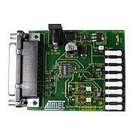
ATA6826-DK Atmel, ATA6826-DK Datasheet - Page 8
ATA6826-DK
Manufacturer Part Number
ATA6826-DK
Description
BOARD EVALUATION FOR ATA6826
Manufacturer
Atmel
Specifications of ATA6826-DK
Main Purpose
Power Management, Half H-Bridge Driver (Internal FET)
Embedded
No
Utilized Ic / Part
ATA6826
Primary Attributes
3 Half H-Bridge Drivers, 1A, 2 kV ESD Protection
Secondary Attributes
Short-Circuit, Thermal & Undervoltage Protection
Lead Free Status / RoHS Status
Contains lead / RoHS non-compliant


7. Noise and Surge Immunity
8. Electrical Characteristics
7.5V < V
8
*) Type means: A =100% tested, B = 100% correlation tested, C = Characterized on samples, D = Design parameter
Note:
Parameters
Conducted interferences
Interference suppression
ESD (Human Body Model)
CDM (Charged Device Model)
MM (Machine Model)
Note:
2.3a
2.3b
No.
1.1
1.2
1.3
1.4
1.5
1.6
2.1
2.2
2.4
2.5
3.1
3.2
1
2
3
VS
1. Delay time between rising edge of the input signal at pin CS after data transmission and switch on output stages to 90% of
Parameters
Current Consumption
Quiescent current VS
Quiescent current VCC
Supply current VS
Supply current VCC
Discharge current VS
Discharge current VS
Undervoltage Detection, Power-on Reset
Power-on reset
threshold
Power-on reset
delay time
Undervoltage-detection
threshold (down)
Undervoltage-detection
threshold (up)
Undervoltage-detection
hysteresis
Undervoltage-detection
delay time
Thermal Prewarning and Shutdown
Thermal prewarning set
Thermal prewarning
reset
Test pulse 5: V
Atmel ATA6826
< 40V; 4.75V < V
final level. Device not in standby for t > 1ms
smax
VCC
= 40V
< 5.25V; INH = High; –40°C < T
Test Conditions
V
4.75V < V
INH = low
V
operating, all outputs off
4.75V < V
normal operating
V
INH = low
V
INH = low
After switching on V
V
V
V
VS
VS
VS
VS
CC
CC
CC
< 20V, INH = low
< 20V normal
= 32.5V,
= 40V,
= 5V
= 5V
= 5V
VCC
VCC
< 5.25V,
< 5.25V,
Test Conditions
ISO 7637-1
VDE 0879 Part 2
ESD STM 5.1
AEC-Q100
ESD STM 5.2
CC
Pin
11
11
11
3
3
3
3
3
3
3
j
< 150 C; unless otherwise specified, all values refer to GND pins.
T
Symbol
T
jPW reset
V
jPW set
I
I
t
V
V
t
I
VCC
I
VCC
I
I
dPor
dUV
V
VCC
VS
VS
VS
VS
Uv
Uv
Uv
Min.
120
105
0.5
2.5
3.2
5.6
6.0
30
10
Typ.
350
145
130
3.9
0.6
15
95
1
4
Max.
500
190
170
155
5.5
4.4
6.5
7.0
25
10
40
2
6
500V all other pins
750V corner pins
Level 4
Level 5
Value
200V
2kV
Unit
mA
mA
mA
µA
µA
µA
°C
°C
µs
µs
V
V
V
V
4834G–BCD–01/11
(1)
Type*
A
A
A
A
A
A
A
A
A
A
A
A
B
B
Related parts for ATA6826-DK
Image
Part Number
Description
Manufacturer
Datasheet
Request
R

Part Number:
Description:
Triple Half-bridge DMOS Output Driver with Serial Input Control
Manufacturer:
ATMEL Corporation
Datasheet:

Part Number:
Description:
MOSFET & Power Driver ICs Triple Half-Bridge Driver
Manufacturer:
Atmel
Datasheet:
Part Number:
Description:
MOSFET & Power Driver ICs Triple Half-Bridge Driver
Manufacturer:
Atmel
Datasheet:

Part Number:
Description:
DEV KIT FOR AVR/AVR32
Manufacturer:
Atmel
Datasheet:
Part Number:
Description:
INTERVAL AND WIPE/WASH WIPER CONTROL IC WITH DELAY
Manufacturer:
ATMEL Corporation
Datasheet:
Part Number:
Description:
Low-Voltage Voice-Switched IC for Hands-Free Operation
Manufacturer:
ATMEL Corporation
Datasheet:
Part Number:
Description:
MONOLITHIC INTEGRATED FEATUREPHONE CIRCUIT
Manufacturer:
ATMEL Corporation
Datasheet:
Part Number:
Description:
AM-FM Receiver IC U4255BM-M
Manufacturer:
ATMEL Corporation
Datasheet:
Part Number:
Description:
Monolithic Integrated Feature Phone Circuit
Manufacturer:
ATMEL Corporation
Datasheet:
Part Number:
Description:
Multistandard Video-IF and Quasi Parallel Sound Processing
Manufacturer:
ATMEL Corporation
Datasheet:
Part Number:
Description:
High-performance EE PLD
Manufacturer:
ATMEL Corporation
Datasheet:
Part Number:
Description:
8-bit Flash Microcontroller
Manufacturer:
ATMEL Corporation
Datasheet: