EVAL-ADUM4160EBZ Analog Devices Inc, EVAL-ADUM4160EBZ Datasheet - Page 11
EVAL-ADUM4160EBZ
Manufacturer Part Number
EVAL-ADUM4160EBZ
Description
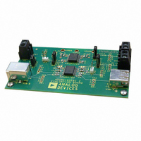
EVALUATION MODULE FOR ADUM4160
Manufacturer
Analog Devices Inc
Series
iCoupler®r
Datasheets
1.ADUM4160BRWZ-RL.pdf
(16 pages)
2.EVAL-ADUM4160EBZ.pdf
(8 pages)
3.EVAL-ADUM4160EBZ.pdf
(14 pages)
Specifications of EVAL-ADUM4160EBZ
Main Purpose
Interface, Digital Isolator
Embedded
No
Utilized Ic / Part
ADuM4160
Primary Attributes
USB Bidirectional Isolation
Secondary Attributes
3.1 V ~ 5.5 V Supply
Silicon Manufacturer
Analog Devices
Application Sub Type
USB Port Isolator
Kit Application Type
Interface
Silicon Core Number
ADuM4160
Lead Free Status / RoHS Status
Lead free / RoHS Compliant
Lead Free Status / RoHS Status
Lead free / RoHS Compliant, Lead free / RoHS Compliant
Other names
Q4508819


Preliminary Technical Data
present on each side, V
connected to V
the coupler. If 3.3V is available, it can be provided to both V
and V
directly from the 3.3V supply.
Figure 5, shows how a typical application is connected if the
upstream side of the coupler was getting power directly from
the USB bus and the downstream side was receiving 3.3V from
the peripheral power supply.
PC BOARD LAYOUT
The ADuM4160 digital isolator requires no external interface
circuitry for the logic interfaces. For full speed operation the
D+ and D- line on each side of the device require a 24Ω
series termination resistor. These resistors are not required for
low speed applications. Power supply bypassing is required at
the input and output supply pins (Figure 5). Install bypass
capacitors between V
capacitor value should have a minimum value of 0.1 μF and low
ESR. The total lead length between both ends of the capacitor
and the power supply pin should not exceed 10 mm . Bypassing
between Pin 2 and Pin 8 and between Pin 9 and Pin 15 should
also be considered, unless the ground pair on each package side
is connected close to the package.
In applications involving high common-mode transients, care
should be taken to ensure that board coupling across the isolation
barrier is minimized. Furthermore, the board layout should be
designed such that any coupling that does occur equally affects
all pins on a given component side. Failure to ensure this could
cause voltage differentials between pins exceeding the device’s
Absolute Maximum Ratings, thereby leading to latch-up or
permanent damage.
DC CORRECTNESS AND MAGNETIC FIELD
IMMUNITY
Positive and negative logic transitions at the isolator input
cause narrow (~1 ns) pulses to be sent to the decoder via the
transformer. The decoder is bistable and is, therefore, either set
or reset by the pulses, indicating input logic transitions. In the
absence of logic transitions at the input for more than ~1 μs, a
periodic set of refresh pulses indicative of the correct input state
are sent to ensure dc correctness at the output. If the decoder
receives no internal pulses of more than about 5 μs, the input
DDx
. This disables the regulator and powers the coupler
Figure 5. Recommended Printed Circuit Board Layout
BUSx
and the internal regulator makes 3.3V to run
BUSx
BUSx
and V
and V
DDx
DDx
on each side of the chip. The
. If 5V is available, it is
±
1%
Rev. Pr F | Page 11 of 14
BUSx
side is assumed to be unpowered or nonfunctional, in which
case the isolator output is forced to a default state (see Table 10)
by the watchdog timer circuit.
The limitation on the ADuM4160’s magnetic field immunity is
set by the condition in which induced voltage in the transformer’s
receiving coil is sufficiently large to either falsely set or reset the
decoder. The following analysis defines the conditions under
which this may occur. The 3 V operating condition of the
ADuM4160 is examined because it represents the most
susceptible mode of operation.
The pulses at the transformer output have an amplitude greater
than 1.0 V. The decoder has a sensing threshold at about 0.5 V, thus
establishing a 0.5 V margin in which induced voltages can be
tolerated. The voltage induced across the receiving coil is given by
where:
β is magnetic flux density (gauss).
N is the number of turns in the receiving coil.
r
Given the geometry of the receiving coil in the ADuM4160 and
an imposed requirement that the induced voltage be at most
50% of the 0.5 V margin at the decoder, a maximum allowable
magnetic field is calculated as shown in Figure 6.
For example, at a magnetic field frequency of 1 MHz, the
maximum allowable magnetic field of 0.2 kgauss induces a
voltage of 0.25 V at the receiving coil. This is about 50% of the
sensing threshold and does not cause a faulty output transition.
Similarly, if such an event were to occur during a transmitted
pulse (and was of the worst-case polarity), it would reduce the
received pulse from >1.0 V to 0.75 V—still well above the 0.5 V
sensing threshold of the decoder.
The preceding magnetic flux density values correspond to
specific current magnitudes at given distances from the
ADuM4160 transformers. Figure 7 expresses these allowable
current magnitudes as a function of frequency for selected
distances. As shown, the ADuM4160 is extremely immune and
can be affected only by extremely large currents operated at
n
is the radius of the n
V = (−dβ/dt)
0.001
Figure 6. Maximum Allowable External Magnetic Flux Density
0.01
100
0.1
10
1
1k
∑
10k
∏r
MAGNETIC FIELD FREQUENCY (Hz)
n
th
2
; n = 1, 2, … , N
turn in the receiving coil (cm).
100k
1M
10M
ADuM4160
100M
Related parts for EVAL-ADUM4160EBZ
Image
Part Number
Description
Manufacturer
Datasheet
Request
R

Part Number:
Description:
EVAL BD For QSOP & SOIC16 Dig Isolators
Manufacturer:
Analog Devices Inc
Datasheet:

Part Number:
Description:
IC, ADJ LDO REG, 1.5V TO 5V 250mA MSOP-8
Manufacturer:
Vishay
Datasheet:

Part Number:
Description:
IC, ADJ LDO REG, 1.5V TO 5V 0.6A 8-TSSOP
Manufacturer:
Vishay
Datasheet:
Part Number:
Description:
IC, ADJ LDO REG, 1.5V TO 5V 250mA MSOP-8
Manufacturer:
Vishay
Datasheet:

Part Number:
Description:
IC ADJ LDO REG 1.5V TO 5V 150mA 5-SOT-23
Manufacturer:
Vishay
Datasheet:

Part Number:
Description:
BOARD EVAL AS1324-AD
Manufacturer:
austriamicrosystems
Datasheet:
Part Number:
Description:
IC, ADJ LDO REG, 1.5V TO 5V 0.6A 8-TSSOP
Manufacturer:
Vishay
Datasheet:

Part Number:
Description:
IC, ADJ LDO REG, 1.5V TO 5V, 0.3A, MSOP8
Manufacturer:
Vishay
Datasheet:
Part Number:
Description:
IC, ADJ LDO REG, 1.5V TO 5V, 0.3A, MSOP8
Manufacturer:
Vishay
Datasheet:
Part Number:
Description:
IC, ADJ LDO REG 1.215V TO 5V 0.3A MSOP-8
Manufacturer:
Vishay
Datasheet:

Part Number:
Description:
±1.7g Dual-Axis IMEMS Accelerometer Evaluation Board
Manufacturer:
Analog Devices Inc
Datasheet:

Part Number:
Description:
IC MULTIPLIER ANALOG 8-SOIC T/R
Manufacturer:
Analog Devices Inc
Datasheet:
Part Number:
Description:
IC ANALOG MULTIPLIER 8-DIP
Manufacturer:
Analog Devices Inc
Datasheet:
Part Number:
Description:
IC ANALOG MULTIPLIER 8-SOIC
Manufacturer:
Analog Devices Inc
Datasheet:
Part Number:
Description:
IC ANALOG MULTIPLIER 8-DIP
Manufacturer:
Analog Devices Inc
Datasheet: