EVAL-ADUM4160EBZ Analog Devices Inc, EVAL-ADUM4160EBZ Datasheet - Page 3
EVAL-ADUM4160EBZ
Manufacturer Part Number
EVAL-ADUM4160EBZ
Description
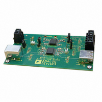
EVALUATION MODULE FOR ADUM4160
Manufacturer
Analog Devices Inc
Series
iCoupler®r
Datasheets
1.ADUM4160BRWZ-RL.pdf
(16 pages)
2.EVAL-ADUM4160EBZ.pdf
(8 pages)
3.EVAL-ADUM4160EBZ.pdf
(14 pages)
Specifications of EVAL-ADUM4160EBZ
Main Purpose
Interface, Digital Isolator
Embedded
No
Utilized Ic / Part
ADuM4160
Primary Attributes
USB Bidirectional Isolation
Secondary Attributes
3.1 V ~ 5.5 V Supply
Silicon Manufacturer
Analog Devices
Application Sub Type
USB Port Isolator
Kit Application Type
Interface
Silicon Core Number
ADuM4160
Lead Free Status / RoHS Status
Lead free / RoHS Compliant
Lead Free Status / RoHS Status
Lead free / RoHS Compliant, Lead free / RoHS Compliant
Other names
Q4508819


Preliminary Technical Data
SPECIFICATIONS
ELECTRICAL CHARACTERISTICS
4.0 V ≤ V
recommended operation range, unless otherwise noted; all typical specifications are at T
relative to their respective ground.
Table 1.
Parameter
DC SPECIFICATIONS
SWITCHING SPECIFICATIONS, I/O pins Low speed
SWITCHING SPECIFICATIONS, I/O pins Full speed
ADuM4160, Total Supply Current
For All Operating Modes
1.5 Mbps
12 Mbps
Input Currents
Single Ended Logic High Input Threshold
Single Ended Logic Low Input Threshold
Logic High Output Voltages
Logic Low Output Voltages
Data Rate
Propagation Delay
Side 1 Output Rise/Fall Time (10% to 90%) Low
Speed
Side 2 Output Rise/Fall Time (10% to 90%) Low
Speed
Low Speed Differential Jitter – Next Transition
Maximum Data Rate
Propagation Delay
Output Rise/Fall Time (10% to 90%) Full Speed
Full Speed Differential Jitter – Next Transition
Idle Current
Single Ended Input Hysteresis
Differential Input Sensitivity
Differential Common Mode Voltage Range
V
V
Transceiver capacitance
Capacitance Matching
Full Speed Driver Impedance
Impedance Matching
Low Speed Differential Jitter – Paired Transition
Full Speed Differential Jitter – Paired Transition
DD1
BUS1
V
V
V
V
V
DD1
DD2
DD1
DD2
DD1
BUS1
and V
and V
or V
or V
or V
or V
or V
≤ 5.5 V, 4.0 V ≤ V
2
DD2
BUS1
BUS2
BUS1
BUS2
BUS1
BUS2
Supply Under Voltage Lockout
Supply Current
Supply Current
Supply Current
Supply Current
Idle Current
Supply Under Voltage Lockout
3
5
4
BUS2
1
≤ 5.5 V; 3.0 V ≤ V
DD1
Symbol
I
I
I
I
I
I
I
I
I
V
V
V
V
V
V
V
V
V
C
Z
t
t
t
|t
|t
t
t
|t
|t
DD1 (L)
DD2 (L)
DD1 (F)
DD2 (F)
DD1 (I)
DD-
UD+
SPD
PDEN
PHL
RF
RF
PHL
RL
IH
IL
HST
DI
CM
OH
OL
UVLO
UVLOB
IN
OUTH
LJN
LJP
HJN
HJP
/t
/t
/t
, I
, I
≤ 3.6 V, 3.0 V ≤ V
, t
, t
,I
|
|
|
|
FF
FF
FL
UD-
DD+
PIN
PLH
PLH
Rev. Pr F | Page 3 of 14
,
, I
,
SPU,
Min
−1
2.0
0.4
0.2
0.8
2.8
0
2.5
3.6
4
75
75
12
20
4
DD2
Typ
5
5
6
6
1.7
+0.1
10
10
1.5
45
15
60
3
1
≤ 3.6 V. All min/max specifications apply over the entire
Max
750
7
7
8
8
2.5
+1
0.8
0.7V
2.5
3.6
0.3
3.0
4.3
20
10
325
300
300
20
A
= 25°C, V
Unit
mA
mA
mA
mA
pF
Mbps C
ns
ns
ns
ns
ns
Mbps C
ns
ns
ns
ns
mA
μA
V
V
V
V
V
V
%
Ω
%
DD1
Test Conditions
750kHz logic signal rate C
750kHz logic signal rate C
6 MHz logic signal rate C
6 MHz logic signal rate C
0 V ≤ V
V
|V
R
R
UD+, UD-, DD+, DD- to ground
C
C
C
C
C
C
C
C
C
= V
SPU,
L
L
L
L
L
L
L
L
L
L
L
L
L
XD+
=15kΩ V
=1.5kΩ V
= 50 pF
= 50 pF
= 200 pF SPD=SPU=low
= 450 pF SPD=SPU=low
= 50 pF,
= 50 pF,
= 50 pF
= 50 pF
= 50 pF SPD=SPU=high
= 50 pF,
= 50 pF,
V
DD2
- V
PDEN
DD-
XD-
= 3.3 V. All voltages are
, V
≤ 3.0
|
L
L
=0V
DD+
=3.6V
, V
UD+
ADuM4160
,V
UD-
, V
L
L
=50pF
=50pF
L
L
SPD
=450pF
=450pF
, V
PIN
,
Related parts for EVAL-ADUM4160EBZ
Image
Part Number
Description
Manufacturer
Datasheet
Request
R

Part Number:
Description:
EVAL BD For QSOP & SOIC16 Dig Isolators
Manufacturer:
Analog Devices Inc
Datasheet:

Part Number:
Description:
IC, ADJ LDO REG, 1.5V TO 5V 250mA MSOP-8
Manufacturer:
Vishay
Datasheet:

Part Number:
Description:
IC, ADJ LDO REG, 1.5V TO 5V 0.6A 8-TSSOP
Manufacturer:
Vishay
Datasheet:
Part Number:
Description:
IC, ADJ LDO REG, 1.5V TO 5V 250mA MSOP-8
Manufacturer:
Vishay
Datasheet:

Part Number:
Description:
IC ADJ LDO REG 1.5V TO 5V 150mA 5-SOT-23
Manufacturer:
Vishay
Datasheet:

Part Number:
Description:
BOARD EVAL AS1324-AD
Manufacturer:
austriamicrosystems
Datasheet:
Part Number:
Description:
IC, ADJ LDO REG, 1.5V TO 5V 0.6A 8-TSSOP
Manufacturer:
Vishay
Datasheet:

Part Number:
Description:
IC, ADJ LDO REG, 1.5V TO 5V, 0.3A, MSOP8
Manufacturer:
Vishay
Datasheet:
Part Number:
Description:
IC, ADJ LDO REG, 1.5V TO 5V, 0.3A, MSOP8
Manufacturer:
Vishay
Datasheet:
Part Number:
Description:
IC, ADJ LDO REG 1.215V TO 5V 0.3A MSOP-8
Manufacturer:
Vishay
Datasheet:

Part Number:
Description:
±1.7g Dual-Axis IMEMS Accelerometer Evaluation Board
Manufacturer:
Analog Devices Inc
Datasheet:

Part Number:
Description:
IC MULTIPLIER ANALOG 8-SOIC T/R
Manufacturer:
Analog Devices Inc
Datasheet:
Part Number:
Description:
IC ANALOG MULTIPLIER 8-DIP
Manufacturer:
Analog Devices Inc
Datasheet:
Part Number:
Description:
IC ANALOG MULTIPLIER 8-SOIC
Manufacturer:
Analog Devices Inc
Datasheet:
Part Number:
Description:
IC ANALOG MULTIPLIER 8-DIP
Manufacturer:
Analog Devices Inc
Datasheet: