AD9520-1/PCBZ Analog Devices Inc, AD9520-1/PCBZ Datasheet - Page 6
AD9520-1/PCBZ
Manufacturer Part Number
AD9520-1/PCBZ
Description
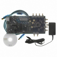
BOARD EVAL FOR AD9520-1
Manufacturer
Analog Devices Inc
Specifications of AD9520-1/PCBZ
Design Resources
Synchronizing Multiple AD9910 1 GSPS Direct Digital Synthesizers (CN0121) Phase Coherent FSK Modulator (CN0186)
Main Purpose
Timing, Clock Generator
Embedded
No
Utilized Ic / Part
AD9520-1
Primary Attributes
12 LVPECL/24 CMOS Output Clock Generator with 2.5 GHz VCO
Secondary Attributes
SPI and I2C Compatible Control Port
Silicon Manufacturer
Analog Devices
Application Sub Type
PLL Clock Synthesizer
Kit Application Type
Clock & Timing
Silicon Core Number
AD9520-0, AD9520-2, AD9520-2
Silicon Family Name
AD9520-X
Rohs Compliant
Yes
Lead Free Status / RoHS Status
Lead free / RoHS Compliant


UG-076
6.
7.
8.
9.
10. Set the VCO divider by clicking the green VCO box in the
Program the R (reference) divider by clicking the
R DIVIDER box at the top of the main window.
Set the desired value and click OK (see Figure 13).
Program the N (feedback) divider by clicking the
N DIVIDER box at the top of the main window.
Set the desired value and click OK. For this example,
N = 5500 can use 8/9 dual modulus mode with A = 4
and B = 687.
Set the charge pump current (1.2 mA in this case) by
clicking the CHARGE PUMP box in the upper right
corner of the main window, and click OK.
Note that if the desired configuration has the phase
detector frequency above 50 MHz, an antibacklash
pulse width of 1.3 ns may work better. This setting is
accessed by clicking the PFD box to the left of the
CHARGE PUMP box. However, this setting normally
does not need to be modified.
center of the main window immediately to the left of the
Cal VCO button.
Rev. 0 | Page 6 of 16
11. Power down unused drivers by clicking the numbered
12. Set the channel dividers by clicking DIVIDER 0 through
13. Click the flashing red WRITE button under the REGISTER
14. Click the blinking yellow Cal VCO button to load the
triangular symbol (see Figure 7) on the right side of the
main window, and then clicking Safe Power Down.
DIVIDER 3, and entering the divider ratio.
W/R section. This loads the desired settings to the AD9520
evaluation board.
VCO calibration window. The default VCO divide ratio
(16) works for all applications. Click the Cal VCO button
in the Calibrate VCO window to begin calibration (see
Figure 19). The PLL should now be locked and the lock
detect (LD) LED on the left side of the board should be on.
Evaluation Board User Guide
Figure 7. Driver Symbol
Related parts for AD9520-1/PCBZ
Image
Part Number
Description
Manufacturer
Datasheet
Request
R

Part Number:
Description:
12/24 Channel Clock Gen 2,0GH
Manufacturer:
Analog Devices Inc
Datasheet:

Part Number:
Description:
12/24 Channel Clock Gen 2,0GH
Manufacturer:
Analog Devices Inc
Datasheet:
Part Number:
Description:
12/24 Channel Clock Gen 2,0GH
Manufacturer:
Analog Devices Inc
Datasheet:
Part Number:
Description:
12/24 Channel Clock Gen 2,0GH
Manufacturer:
Analog Devices Inc
Datasheet:
Part Number:
Description:
12/24 Channel Clock Gen 2,0GH
Manufacturer:
Analog Devices Inc
Datasheet:
Part Number:
Description:
Clock IC With 2.8GHz On-chip VCO
Manufacturer:
Analog Devices Inc
Datasheet:
Part Number:
Description:
Lock IC With 2.8GHz On-chip VCO
Manufacturer:
Analog Devices Inc
Datasheet:
Part Number:
Description:
12/24 Channel Clock Gen 2,5 GHz VCO
Manufacturer:
Analog Devices Inc
Datasheet:
Part Number:
Description:
12/24 Channel Clock Distribution W/ On-C
Manufacturer:
Analog Devices Inc
Datasheet:
Part Number:
Description:
12/24 Channel Clock Gen 2,25GH
Manufacturer:
Analog Devices Inc
Datasheet:
Part Number:
Description:
12/24 Channel Clock Distribution W/ On-C
Manufacturer:
Analog Devices Inc
Datasheet:
Part Number:
Description:
12/24 Channel Clock Distribution W/ On-C
Manufacturer:
Analog Devices Inc
Datasheet:
Part Number:
Description:
Clock IC With 1.6GHz On-chip VCO
Manufacturer:
Analog Devices Inc
Datasheet:
Part Number:
Description:
Clock IC With 1.6GHz On-chip VCO
Manufacturer:
Analog Devices Inc
Datasheet:
Part Number:
Description:
12/24-Output Clock Generator
Manufacturer:
Analog Devices Inc
Datasheet: