AD9520-1/PCBZ Analog Devices Inc, AD9520-1/PCBZ Datasheet - Page 12
AD9520-1/PCBZ
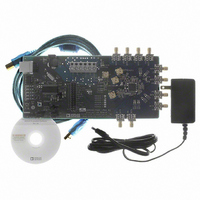
Manufacturer Part Number
AD9520-1/PCBZ
Description
BOARD EVAL FOR AD9520-1
Manufacturer
Analog Devices Inc
Specifications of AD9520-1/PCBZ
Design Resources
Synchronizing Multiple AD9910 1 GSPS Direct Digital Synthesizers (CN0121) Phase Coherent FSK Modulator (CN0186)
Main Purpose
Timing, Clock Generator
Embedded
No
Utilized Ic / Part
AD9520-1
Primary Attributes
12 LVPECL/24 CMOS Output Clock Generator with 2.5 GHz VCO
Secondary Attributes
SPI and I2C Compatible Control Port
Silicon Manufacturer
Analog Devices
Application Sub Type
PLL Clock Synthesizer
Kit Application Type
Clock & Timing
Silicon Core Number
AD9520-0, AD9520-2, AD9520-2
Silicon Family Name
AD9520-X
Rohs Compliant
Yes
Lead Free Status / RoHS Status
Lead free / RoHS Compliant


AD9520-1
CLOCK OUTPUT ABSOLUTE TIME JITTER (CLOCK GENERATION USING EXTERNAL VCXO)
Table 10.
Parameter
LVPECL OUTPUT ABSOLUTE TIME JITTER
CLOCK OUTPUT ADDITIVE TIME JITTER (VCO DIVIDER NOT USED)
Table 11.
Parameter
LVPECL OUTPUT ADDITIVE TIME JITTER
CMOS OUTPUT ADDITIVE TIME JITTER
LVPECL = 245.76 MHz; PLL LBW = 125 Hz
LVPECL = 122.88 MHz; PLL LBW = 125 Hz
LVPECL = 61.44 MHz; PLL LBW = 125 Hz
CLK = 622.08 MHz
CLK = 622.08 MHz
CLK = 1000 MHz
CLK = 500 MHz
CLK = 200 MHz
Any LVPECL Output = 622.08 MHz
Divide Ratio = 1
Any LVPECL Output = 155.52 MHz
Divide Ratio = 4
Any LVPECL Output = 100 MHz
Divide Ratio = 10
Any LVPECL Output = 100 MHz
Divide Ratio = 5
Any CMOS Output Pair = 100 MHz
Divide Ratio = 2
Min
Min
Typ
54
77
109
79
114
163
124
176
259
Rev. 0 | Page 12 of 84
Typ
46
64
223
209
325
Max
Max
Unit
fs rms
fs rms
fs rms
fs rms
fs rms
fs rms
fs rms
fs rms
fs rms
Unit
fs rms
fs rms
fs rms
fs rms
fs rms
Test Conditions/Comments
Application example based on a typical setup using an
external 245.76 MHz VCXO (Toyocom TCO-2112);
reference = 15.36 MHz; R DIV = 1
Integration BW = 200 kHz to 5 MHz
Integration BW = 200 kHz to 10 MHz
Integration BW = 12 kHz to 20 MHz
Integration BW = 200 kHz to 5 MHz
Integration BW = 200 kHz to 10 MHz
Integration BW = 12 kHz to 20 MHz
Integration BW = 200 kHz to 5 MHz
Integration BW = 200 kHz to 10 MHz
Integration BW = 12 kHz to 20 MHz
Test Conditions/Comments
Distribution section only; does not include
PLL and VCO; measured at rising edge of
clock signal
Integration bandwidth = 12 kHz to 20 MHz
Integration bandwidth = 12 kHz to 20 MHz
Calculated from SNR of ADC method
Broadband jitter
Calculated from SNR of ADC method
Broadband jitter
Distribution section only; does not include
PLL and VCO
Calculated from SNR of ADC method
Broadband jitter
Related parts for AD9520-1/PCBZ
Image
Part Number
Description
Manufacturer
Datasheet
Request
R

Part Number:
Description:
12/24 Channel Clock Gen 2,0GH
Manufacturer:
Analog Devices Inc
Datasheet:

Part Number:
Description:
12/24 Channel Clock Gen 2,0GH
Manufacturer:
Analog Devices Inc
Datasheet:
Part Number:
Description:
12/24 Channel Clock Gen 2,0GH
Manufacturer:
Analog Devices Inc
Datasheet:
Part Number:
Description:
12/24 Channel Clock Gen 2,0GH
Manufacturer:
Analog Devices Inc
Datasheet:
Part Number:
Description:
12/24 Channel Clock Gen 2,0GH
Manufacturer:
Analog Devices Inc
Datasheet:
Part Number:
Description:
Clock IC With 2.8GHz On-chip VCO
Manufacturer:
Analog Devices Inc
Datasheet:
Part Number:
Description:
Lock IC With 2.8GHz On-chip VCO
Manufacturer:
Analog Devices Inc
Datasheet:
Part Number:
Description:
12/24 Channel Clock Gen 2,5 GHz VCO
Manufacturer:
Analog Devices Inc
Datasheet:
Part Number:
Description:
12/24 Channel Clock Distribution W/ On-C
Manufacturer:
Analog Devices Inc
Datasheet:
Part Number:
Description:
12/24 Channel Clock Gen 2,25GH
Manufacturer:
Analog Devices Inc
Datasheet:
Part Number:
Description:
12/24 Channel Clock Distribution W/ On-C
Manufacturer:
Analog Devices Inc
Datasheet:
Part Number:
Description:
12/24 Channel Clock Distribution W/ On-C
Manufacturer:
Analog Devices Inc
Datasheet:
Part Number:
Description:
Clock IC With 1.6GHz On-chip VCO
Manufacturer:
Analog Devices Inc
Datasheet:
Part Number:
Description:
Clock IC With 1.6GHz On-chip VCO
Manufacturer:
Analog Devices Inc
Datasheet:
Part Number:
Description:
12/24-Output Clock Generator
Manufacturer:
Analog Devices Inc
Datasheet: