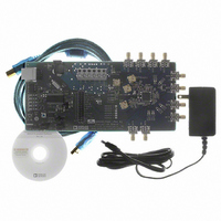
AD9520-1/PCBZ Analog Devices Inc, AD9520-1/PCBZ Datasheet - Page 14

AD9520-1/PCBZ
Manufacturer Part Number
AD9520-1/PCBZ
Description
BOARD EVAL FOR AD9520-1
Manufacturer
Analog Devices Inc
Specifications of AD9520-1/PCBZ
Design Resources
Synchronizing Multiple AD9910 1 GSPS Direct Digital Synthesizers (CN0121) Phase Coherent FSK Modulator (CN0186)
Main Purpose
Timing, Clock Generator
Embedded
No
Utilized Ic / Part
AD9520-1
Primary Attributes
12 LVPECL/24 CMOS Output Clock Generator with 2.5 GHz VCO
Secondary Attributes
SPI and I2C Compatible Control Port
Silicon Manufacturer
Analog Devices
Application Sub Type
PLL Clock Synthesizer
Kit Application Type
Clock & Timing
Silicon Core Number
AD9520-0, AD9520-2, AD9520-2
Silicon Family Name
AD9520-X
Rohs Compliant
Yes
Lead Free Status / RoHS Status
Lead free / RoHS Compliant
AD9520-1
SERIAL CONTROL PORT—I²C MODE
Table 14.
Parameter
SDA, SCL (WHEN INPUTTING DATA)
SDA (WHEN OUTPUTTING DATA)
TIMING
1
According to the original I
falling edge.
Input Logic 1 Voltage
Input Logic 0 Voltage
Input Current with an Input Voltage Between
Hysteresis of Schmitt Trigger Inputs
Pulse Width of Spikes That Must Be Suppressed by
Output Logic 0 Voltage at 3 mA Sink Current
Output Fall Time from VIH
Clock Rate (SCL, f
Bus Free Time Between a Stop and Start Condition, t
Setup Time for a Repeated Start Condition, t
Hold Time (Repeated) Start Condition (After This Period,
Setup Time for Stop Condition, t
Low Period of the SCL Clock, t
High Period of the SCL Clock, t
SCL, SDA Rise Time, t
SCL, SDA Fall Time, t
Data Setup Time, t
Data Hold Time, t
Capacitive Load for Each Bus Line, C
0.1 × VS and 0.9 × VS
the Input Filter, t
Capacitance from 10 pF to 400 pF
the First Clock Pulse Is Generated), t
I2C
HLD; DAT
SET; DAT
SPIKE
)
FALL
2
RISE
C specification, an I
MIN
to VIL
LOW
HIGH
SET; STP
MAX
b
2
C master must also provide a minimum hold time of 300 ns for the SDA signal to bridge the undefined region of the SCL
with a Bus
HLD; STR
SET; STR
IDLE
Rev. 0 | Page 14 of 84
Min
0.7 × VS
−10
0.015 × VS
20 + 0.1 C
1.3
0.6
0.6
0.6
1.3
0.6
20 + 0.1 C
20 + 0.1 C
120
140
b
b
b
Typ
Max
0.3 × VS
+10
50
0.4
250
400
300
300
880
400
Unit
ns
kHz
μs
μs
μs
μs
μs
μs
pF
V
V
μA
V
V
ns
ns
ns
ns
ns
Test Conditions/Comments
(C
Note that all I
referred to VIH
VIL
This is a minor deviation from
the original I²C specification of
100 ns minimum
This is a minor deviation from
the original I²C specification of
0 ns minimum
b
MAX
= capacitance of one bus line in pF)
levels (0.7 × VS)
2
C timing values
MIN
1
(0.3 × VS) and


