ADNK-5033-FS27 Avago Technologies US Inc., ADNK-5033-FS27 Datasheet - Page 5
ADNK-5033-FS27
Manufacturer Part Number
ADNK-5033-FS27
Description
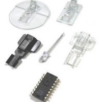
KIT REF DES OPT MOUSE ADNS-5030
Manufacturer
Avago Technologies US Inc.
Datasheets
1.ADNK-5033-FS27.pdf
(24 pages)
2.ADNK-5033-FS27.pdf
(6 pages)
3.ADNK-5033-FS27.pdf
(32 pages)
Specifications of ADNK-5033-FS27
Main Purpose
Reference Design, Optical Mouse
Utilized Ic / Part
ADNS-5030
Wireless Frequency
27 MHz
Interface Type
USB
Modulation
FSK
For Use With/related Products
MC68HC908QY4A, MC68HC908JB12
Lead Free Status / RoHS Status
Lead free / RoHS Compliant
Secondary Attributes
-
Embedded
-
Primary Attributes
-
Lead Free Status / Rohs Status
Lead free / RoHS Compliant


The communication between the sensor and the
MC68HC908QY4A is through a serial peripheral
interface (SPI) with clock input at the SCLK pin, the
data interface at the MISO and MOSI pins.
The receiver consists of:
• The MC68HC908JB12
• A button for identity device (ID) code setting
• A in-circuit programming (ICP) connector
• RF front-end circuitry
The functions of the MC68HC908JB12 are to handle
the USB transactions, capture and process data from
RF receiver front end. The processed data is converted
into USB report format and sent to the host.
Figure 4. MC68HC908JB12-ADNS-5030 Optical Mouse Hardware Block Diagram - Receiver
5
The ID button is used to interrupt the MCU for a new
ID code detection. The MCU will search if there is any
ID code embedded in the RF data packet and store the
new ID in FLASH memory. There is a transistor wakeup
circuit connected at the IRQ pin and is controlled by
an I/O pin. The MCU will configure the wakeup circuit
before entering stop mode for power saving. The RC
components connected at the transistor base input will
be charged up, and eventually turn on the transistor
and pull low the IRQ to wakeup the MCU.
The ICP interface is connected at port A. The ICP is
used for future firmware updating through the Cyclone
Programming Tools.
Related parts for ADNK-5033-FS27
Image
Part Number
Description
Manufacturer
Datasheet
Request
R

Part Number:
Description:
KIT REFERENCE DESIGN ADNK-5030
Manufacturer:
Avago Technologies US Inc.
Datasheet:

Part Number:
Description:
A2700 Sample Kit
Manufacturer:
Avago Technologies US Inc.
Datasheet:

Part Number:
Description:
OPTOCOUPLER GATE DRV 2A 16-SOIC
Manufacturer:
Avago Technologies US Inc.
Datasheet:
Part Number:
Description:
OPTOCOUPLER 2CH 2.5A 16-SOIC
Manufacturer:
Avago Technologies US Inc.
Datasheet:

Part Number:
Description:
OPTOCOUPLER GATE DRV 0.4A 16SOIC
Manufacturer:
Avago Technologies US Inc.
Datasheet:

Part Number:
Description:
OPTOCOUPLER 2.0A 250KHZ 8-DIP
Manufacturer:
Avago Technologies US Inc.
Datasheet:

Part Number:
Description:
OPTOCOUPLER 2.0A 250KHZ GW 8-SMD
Manufacturer:
Avago Technologies US Inc.
Datasheet:

Part Number:
Description:
OPTOCOUPLER 2CH 15MBD 3.3V 8SOIC
Manufacturer:
Avago Technologies US Inc.
Datasheet:
Part Number:
Description:
OPTOCOUPLER DARL-OUT 8-DIP
Manufacturer:
Avago Technologies US Inc.
Datasheet:
Part Number:
Description:
OPTOCOUPLER IGBT DRIVE 0.4A 8DIP
Manufacturer:
Avago Technologies US Inc.
Datasheet:
Part Number:
Description:
OPTOCOUPLER DARL-OUT 8-DIP
Manufacturer:
Avago Technologies US Inc.
Datasheet:

Part Number:
Description:
OPTOCOUPLER 1CH 1MBS 8-SMD GW
Manufacturer:
Avago Technologies US Inc.
Datasheet:
Part Number:
Description:
OPTOCOUPLER GATE DRIVER 8-DIP
Manufacturer:
Avago Technologies US Inc.
Datasheet:

Part Number:
Description:
OPTOCOUPLER GATE DRIVER 8-SMD
Manufacturer:
Avago Technologies US Inc.
Datasheet:

Part Number:
Description:
OPTOCOUPLER PHOTOTRANS 4-SMD
Manufacturer:
Avago Technologies US Inc.
Datasheet: