CDB4271 Cirrus Logic Inc, CDB4271 Datasheet - Page 10
CDB4271
Manufacturer Part Number
CDB4271
Description
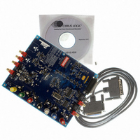
EVAL BOARD CS4271 STEREO CODEC
Manufacturer
Cirrus Logic Inc
Datasheet
1.CDB4271.pdf
(28 pages)
Specifications of CDB4271
Main Purpose
Audio, CODEC
Embedded
Yes, FPGA / CPLD
Utilized Ic / Part
CS4271
Primary Attributes
Stereo, 24-Bit, 192 kHz Sample Rate
Secondary Attributes
I²S, S/PDIF Inputs and Outputs, Analog Inputs and Outputs, GUI
Product
Audio Modules
Lead Free Status / RoHS Status
Contains lead / RoHS non-compliant
Lead Free Status / RoHS Status
Lead free / RoHS Compliant, Contains lead / RoHS non-compliant
Other names
598-1003


10
Header/8416
JUMPER /
MCLK[1:0]
J13, J14,
J15, J20,
SWITCH
J21, J22
M/S[1:0]
J11, J19
Coaxial/
128/256
Optical
I2S/LJ
M[1:0]
(S1)
(S1)
(S1)
(S1)
(S1)
(S1)
(S1)
J10
J9
J8
Selects LED or Mute Circuit for
Digital Interface Format Select
Subclock Master/Slave Select
CS4271 SDIN Source Select
CS4271 Speed Mode Select
Selects source of voltage for
Selects source of voltage for
Selects source of voltage for
Master Clock Source Select
Master Clock Speed Select
Optical or Coaxial S/PDIF
Selects DAC Output Filter
AOUTA, AOUTB
the VL supplies
the VD supply
the VA supply
Input Select
PURPOSE
Table 2. Jumper/Switch Settings
POSITION
+3.3V
+3.3V
*+5V
*+5V
*+5V
ADJ
ADJ
ADJ
*00
*00
*01
01
10
11
01
10
11
00
10
11
*0
*0
*0
*0
*2
*1
1
1
1
1
1
2
CS4271 is Master
CS8416 is Master
CS8406 is Master
PCM Header, J26, is Master
CS8416 Provides MCLK
CS4271 Provides MCLK
PCM Header, J26, Provides MCLK
PCM Header, J26, Provides MCLK
CS8416 Provides SDIIN
PCM Header, J26, Provides SDIN
Optical Input
Coaxial Input
Left Justified, 24-bit
I
256*Fs
128*Fs
Single-Speed Mode, with De-emphasis
Single-Speed Mode, w/out De-emphasis
Double-Speed Mode
Quad-Speed Mode
Mute Circuit Affects Analog Output
Mute Circuit Disconnected (LED displays
xMUTEC status)
Voltage source is J1, +5.0 V binding post
Voltage source is J5, VA binding post
Voltage source is J1, +5V binding post
Voltage source is +3.3 V regulator
Voltage source is J3, VD binding post
Voltage source is J1, +5V binding post
Voltage source is +3.3 V regulator
Voltage source is J2, VL binding post
Selects standard 2-pole filter
Inserts instrumentation-amp and resistor
divider.
2
S, 24-Bit
FUNCTION SELECTED
*Default factory settings
CDB4271
Related parts for CDB4271
Image
Part Number
Description
Manufacturer
Datasheet
Request
R

Part Number:
Description:
Development Kit
Manufacturer:
Cirrus Logic Inc
Datasheet:
Part Number:
Description:
Development Kit
Manufacturer:
Cirrus Logic Inc
Datasheet:


Part Number:
Description:
High-efficiency PFC + Fluorescent Lamp Driver Reference Design
Manufacturer:
Cirrus Logic Inc
Datasheet:
Part Number:
Description:
Development Kit
Manufacturer:
Cirrus Logic Inc
Datasheet:
Part Number:
Description:
Development Kit
Manufacturer:
Cirrus Logic Inc
Datasheet:

Part Number:
Description:
Development Kit
Manufacturer:
Cirrus Logic Inc
Datasheet:
Part Number:
Description:
Development Kit
Manufacturer:
Cirrus Logic Inc
Datasheet:
Part Number:
Description:
Development Kit
Manufacturer:
Cirrus Logic Inc
Datasheet:
Part Number:
Description:
Development Kit
Manufacturer:
Cirrus Logic Inc
Datasheet:

Part Number:
Description:
EVALUATION BOARD FOR CS8427
Manufacturer:
Cirrus Logic Inc
Datasheet:

Part Number:
Description:
BOARD EVAL FOR CS8416 RCVR
Manufacturer:
Cirrus Logic Inc
Datasheet:

Part Number:
Description:
EVALUATION BOARD FOR CS8420
Manufacturer:
Cirrus Logic Inc
Datasheet:

Part Number:
Description:
KIT DEVELOPMENT EP9315 ARM9
Manufacturer:
Cirrus Logic Inc
Datasheet:

Part Number:
Description:
KIT DEVELOPMENT EP9302 ARM9
Manufacturer:
Cirrus Logic Inc
Datasheet: