CDB42448 Cirrus Logic Inc, CDB42448 Datasheet - Page 35
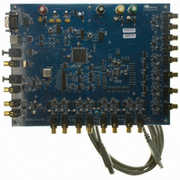
CDB42448
Manufacturer Part Number
CDB42448
Description
BOARD EVAL FOR CS42448 CODEC
Manufacturer
Cirrus Logic Inc
Specifications of CDB42448
Main Purpose
Audio, CODEC
Embedded
Yes, FPGA / CPLD
Utilized Ic / Part
CS42448
Primary Attributes
24-Bit, 192 kHz, 6 ADCs: 102dB Dynamic Range, 8 DACs: 105dB Dynamic Range
Secondary Attributes
Time Division Multiplexed (TDM), I2C, and SPI Interface, Popguard® Technology
Description/function
Audio CODECs
Operating Supply Voltage
5 V to 12 V
Product
Audio Modules
For Use With/related Products
CS42448
Lead Free Status / RoHS Status
Contains lead / RoHS non-compliant
Lead Free Status / RoHS Status
Lead free / RoHS Compliant, Contains lead / RoHS non-compliant
Other names
598-1151


DS648F3
4.6.2
4.7
4.7.1
AUX_LRCK
AUX_SCLK
AUX_SDIN
Control Port Description and Timing
The control port is used to access the registers allowing the CS42448 to be configured for the desired op-
erational modes and formats. The operation of the control port may be completely asynchronous with re-
spect to the audio sample rates. However, to avoid potential interference problems, the control port pins
should remain static if no operation is required.
The control port has two modes: SPI and I²C, with the CS42448 acting as a slave device. SPI Mode is se-
lected if there is a high-to-low transition on the AD0/CS pin, after the RST pin has been brought high. I²C
Mode is selected by connecting the AD0/CS pin through a resistor to VLC or DGND, thereby permanently
selecting the desired AD0 bit address state.
Left-Justified
SPI Mode
In SPI Mode, CS is the CS42448 chip-select signal, CCLK is the control port bit clock (input into the
CS42448 from the microcontroller), CDIN is the input data line from the microcontroller, CDOUT is the
output data line to the microcontroller. Data is clocked in on the rising edge of CCLK and out on the falling
edge.
Figure 23
first seven bits on CDIN form the chip address and must be 1001111. The eighth bit is a read/write indi-
cator (R/W), which should be low to write. The next eight bits form the Memory Address Pointer (MAP),
which is set to the address of the register that is to be updated. The next eight bits are the data which will
be placed into the register designated by the MAP. During writes, the CDOUT output stays in the Hi-Z
state. It may be externally pulled high or low with a 47 kΩ resistor, if desired.
There is a MAP auto-increment capability, enabled by the INCR bit in the MAP register. If INCR is a zero,
the MAP will stay constant for successive read or writes. If INCR is set to a 1, the MAP will auto-increment
after each byte is read or written, allowing block reads or writes of successive registers.
To read a register, the MAP has to be set to the correct address by executing a partial write cycle which
finishes (CS high) immediately after the MAP byte. The MAP auto-increment bit (INCR) may be set or not,
as desired. To begin a read, bring CS low, send out the chip address and set the read/write bit (R/W) high.
The next falling edge of CCLK will clock out the MSB of the addressed register (CDOUT will leave the high
impedance state). If the MAP auto-increment bit is set to 1, the data for successive registers will appear
consecutively.
M S B
shows the operation of the control port in SPI Mode. To write to a register, bring CS low. The
L e ft C h a n n el
AUX1
Figure 22. AUX Left-Justified Format
L S B
M S B
R ig ht C h a n n el
AUX2
L S B
CS42448
MSB
35
Related parts for CDB42448
Image
Part Number
Description
Manufacturer
Datasheet
Request
R

Part Number:
Description:
Development Kit
Manufacturer:
Cirrus Logic Inc
Datasheet:
Part Number:
Description:
Development Kit
Manufacturer:
Cirrus Logic Inc
Datasheet:


Part Number:
Description:
High-efficiency PFC + Fluorescent Lamp Driver Reference Design
Manufacturer:
Cirrus Logic Inc
Datasheet:
Part Number:
Description:
Development Kit
Manufacturer:
Cirrus Logic Inc
Datasheet:
Part Number:
Description:
Development Kit
Manufacturer:
Cirrus Logic Inc
Datasheet:

Part Number:
Description:
Development Kit
Manufacturer:
Cirrus Logic Inc
Datasheet:
Part Number:
Description:
Development Kit
Manufacturer:
Cirrus Logic Inc
Datasheet:
Part Number:
Description:
Development Kit
Manufacturer:
Cirrus Logic Inc
Datasheet:
Part Number:
Description:
Development Kit
Manufacturer:
Cirrus Logic Inc
Datasheet:

Part Number:
Description:
EVALUATION BOARD FOR CS8427
Manufacturer:
Cirrus Logic Inc
Datasheet:

Part Number:
Description:
BOARD EVAL FOR CS8416 RCVR
Manufacturer:
Cirrus Logic Inc
Datasheet:

Part Number:
Description:
EVALUATION BOARD FOR CS8420
Manufacturer:
Cirrus Logic Inc
Datasheet:

Part Number:
Description:
KIT DEVELOPMENT EP9315 ARM9
Manufacturer:
Cirrus Logic Inc
Datasheet:

Part Number:
Description:
KIT DEVELOPMENT EP9302 ARM9
Manufacturer:
Cirrus Logic Inc
Datasheet: