CDB42448 Cirrus Logic Inc, CDB42448 Datasheet - Page 5
CDB42448
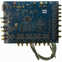
Manufacturer Part Number
CDB42448
Description
BOARD EVAL FOR CS42448 CODEC
Manufacturer
Cirrus Logic Inc
Specifications of CDB42448
Main Purpose
Audio, CODEC
Embedded
Yes, FPGA / CPLD
Utilized Ic / Part
CS42448
Primary Attributes
24-Bit, 192 kHz, 6 ADCs: 102dB Dynamic Range, 8 DACs: 105dB Dynamic Range
Secondary Attributes
Time Division Multiplexed (TDM), I2C, and SPI Interface, Popguard® Technology
Description/function
Audio CODECs
Operating Supply Voltage
5 V to 12 V
Product
Audio Modules
For Use With/related Products
CS42448
Lead Free Status / RoHS Status
Contains lead / RoHS non-compliant
Lead Free Status / RoHS Status
Lead free / RoHS Compliant, Contains lead / RoHS non-compliant
Other names
598-1151


CS42448
Figure 37.DSM Transition Band ................................................................................................................ 57
Figure 38.DSM Transition Band (Detail) ................................................................................................... 58
Figure 39.DSM Passband Ripple .............................................................................................................. 58
Figure 40.QSM Stopband Rejection ......................................................................................................... 58
Figure 41.QSM Transition Band ................................................................................................................ 58
Figure 42.QSM Transition Band (Detail) ................................................................................................... 58
Figure 43.QSM Passband Ripple .............................................................................................................. 58
Figure 44.SSM Stopband Rejection .......................................................................................................... 59
Figure 45.SSM Transition Band ................................................................................................................ 59
Figure 46.SSM Transition Band (detail) .................................................................................................... 59
Figure 47.SSM Passband Ripple .............................................................................................................. 59
Figure 48.DSM Stopband Rejection .......................................................................................................... 59
Figure 49.DSM Transition Band ................................................................................................................ 59
Figure 50.DSM Transition Band (detail) .................................................................................................... 60
Figure 51.DSM Passband Ripple .............................................................................................................. 60
Figure 52.QSM Stopband Rejection ......................................................................................................... 60
Figure 53.QSM Transition Band ................................................................................................................ 60
Figure 54.QSM Transition Band (detail) .................................................................................................... 60
Figure 55.QSM Passband Ripple .............................................................................................................. 60
LIST OF TABLES
Table 1. I/O Power Rails ............................................................................................................................. 8
Table 2. Single-Speed Mode Common Frequencies ................................................................................ 30
Table 3. Double-Speed Mode Common Frequencies ............................................................................... 30
Table 4. Quad-Speed Mode Common Frequencies ................................................................................. 30
Table 5. I²S, LJ, RJ Clock Ratios .............................................................................................................. 31
Table 6. OLM#1 Clock Ratios ................................................................................................................... 31
Table 7. OLM#2 Clock Ratios ................................................................................................................... 31
Table 8. TDM Clock Ratios ....................................................................................................................... 31
Table 9. Serial Audio Interface Channel Allocations ................................................................................. 34
Table 10. MCLK Frequency Settings for I²S, Left and Right Justified Interface Formats .......................... 43
Table 12. DAC Digital Interface Formats .................................................................................................. 44
Table 11. MCLK Frequency Settings for TDM & OLM Interface Formats ................................................. 44
Table 13. ADC Digital Interface Formats .................................................................................................. 45
Table 14. Example AOUT Volume Settings .............................................................................................. 49
Table 15. Example AIN Volume Settings .................................................................................................. 50
DS648F3
5
Related parts for CDB42448
Image
Part Number
Description
Manufacturer
Datasheet
Request
R

Part Number:
Description:
Development Kit
Manufacturer:
Cirrus Logic Inc
Datasheet:
Part Number:
Description:
Development Kit
Manufacturer:
Cirrus Logic Inc
Datasheet:


Part Number:
Description:
High-efficiency PFC + Fluorescent Lamp Driver Reference Design
Manufacturer:
Cirrus Logic Inc
Datasheet:
Part Number:
Description:
Development Kit
Manufacturer:
Cirrus Logic Inc
Datasheet:
Part Number:
Description:
Development Kit
Manufacturer:
Cirrus Logic Inc
Datasheet:

Part Number:
Description:
Development Kit
Manufacturer:
Cirrus Logic Inc
Datasheet:
Part Number:
Description:
Development Kit
Manufacturer:
Cirrus Logic Inc
Datasheet:
Part Number:
Description:
Development Kit
Manufacturer:
Cirrus Logic Inc
Datasheet:
Part Number:
Description:
Development Kit
Manufacturer:
Cirrus Logic Inc
Datasheet:

Part Number:
Description:
EVALUATION BOARD FOR CS8427
Manufacturer:
Cirrus Logic Inc
Datasheet:

Part Number:
Description:
BOARD EVAL FOR CS8416 RCVR
Manufacturer:
Cirrus Logic Inc
Datasheet:

Part Number:
Description:
EVALUATION BOARD FOR CS8420
Manufacturer:
Cirrus Logic Inc
Datasheet:

Part Number:
Description:
KIT DEVELOPMENT EP9315 ARM9
Manufacturer:
Cirrus Logic Inc
Datasheet:

Part Number:
Description:
KIT DEVELOPMENT EP9302 ARM9
Manufacturer:
Cirrus Logic Inc
Datasheet: