KIT34673EPEVBE Freescale Semiconductor, KIT34673EPEVBE Datasheet - Page 9
KIT34673EPEVBE
Manufacturer Part Number
KIT34673EPEVBE
Description
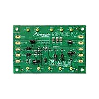
KIT EVALUATION FOR MC34673
Manufacturer
Freescale Semiconductor
Type
Battery Managementr
Specifications of KIT34673EPEVBE
Main Purpose
Power Management, Battery Charger
Embedded
No
Utilized Ic / Part
MC34673
Primary Attributes
1 Cell- Li-Ion
Secondary Attributes
LED Status Indicators
Input Voltage
2.6 V
Maximum Operating Temperature
+ 85 C
Minimum Operating Temperature
- 40 C
Product
Power Management Modules
Supply Current
1.2 A
Silicon Manufacturer
Freescale
Silicon Core Number
MC34673
Kit Application Type
Power Management - Battery
Application Sub Type
Battery Charger
Kit Contents
Evaluation Board, CD
Rohs Compliant
Yes
Lead Free Status / RoHS Status
Lead free / RoHS Compliant
For Use With/related Products
MC34673


IMPORTANT: DO NOT APPLY HIGHER THAN A 12V DC INPUT VOLTAGE TO VIN IF THE
PINS 1 and 2 ARE SHORTED.
The absolute maximum voltage at the PPR and CHG pin is 12V. When applying higher than a
12V input voltage, select the BAT pin to power the LEDs.
The JP3 pin header allows the user to disable the MC34673 when shorting pins 1 and 2. Leaving
it open enables the MC34673.
The JP4 pin header links the BAT pin and the external battery connector. It allows the user to
measure the charging current from the MC34673 into the battery with a current meter between
pins 1 and 2. The default setting is to short pins 1 and 2.
JP5 and JP6 are used to let the user supply an I/O logic voltage to PPR and CHG, so the system
can interface to the PPR and CHG signals with the same voltage level. When using LEDs to
indicate the charging status, leave JP5 and JP6 open. When interfacing the PPR and CHG signal
to the system, short pins 1 and 2 of JP5 and JP6, and leave JP2 open.
JP7 and JP8 set the charge current. The current values related to JP7 and JP8 settings are
shown in
JP9 selects the power supply for pulling up the voltage of the FAST signal. Shorting pins 1 and
2 selects the externally supplied I/O logic voltage. Shorting pins 2 and 3 selects the battery
voltage.
The default configuration of the evaluation board is a standalone charger. The default settings of
the evaluation board are shown in
When using the evaluation board to connect to the system, apply the required I/O logic voltage
at the VL pad of the evaluation board and set the pin header jumpers as shown in
Freescale Semiconductor
Table
Table 3. The Default Settings of the Pin Headers for Standalone Chargers
2.
Using the High Input Voltage Charger for Single Cell Li-Ion
JP1
JP2
JP3
JP4
JP5
JP6
JP7
JP8
JP9
Pin Header Jumpers
Table
3.
Shorted
1 and 2 shorted
Open
Shorted
Open
Open
Shorted
Shorted
1 and 2 shorted
Default Setting
Batteries, Rev. 1.0
Evaluation Board Configuration
Table
4.
9
Related parts for KIT34673EPEVBE
Image
Part Number
Description
Manufacturer
Datasheet
Request
R

Part Number:
Description:
Manufacturer:
Freescale Semiconductor, Inc
Datasheet:
Part Number:
Description:
Manufacturer:
Freescale Semiconductor, Inc
Datasheet:
Part Number:
Description:
Manufacturer:
Freescale Semiconductor, Inc
Datasheet:
Part Number:
Description:
Manufacturer:
Freescale Semiconductor, Inc
Datasheet:
Part Number:
Description:
Manufacturer:
Freescale Semiconductor, Inc
Datasheet:
Part Number:
Description:
Manufacturer:
Freescale Semiconductor, Inc
Datasheet:
Part Number:
Description:
Manufacturer:
Freescale Semiconductor, Inc
Datasheet:
Part Number:
Description:
Manufacturer:
Freescale Semiconductor, Inc
Datasheet:
Part Number:
Description:
Manufacturer:
Freescale Semiconductor, Inc
Datasheet:
Part Number:
Description:
Manufacturer:
Freescale Semiconductor, Inc
Datasheet:
Part Number:
Description:
Manufacturer:
Freescale Semiconductor, Inc
Datasheet:
Part Number:
Description:
Manufacturer:
Freescale Semiconductor, Inc
Datasheet:
Part Number:
Description:
Manufacturer:
Freescale Semiconductor, Inc
Datasheet:
Part Number:
Description:
Manufacturer:
Freescale Semiconductor, Inc
Datasheet:
Part Number:
Description:
Manufacturer:
Freescale Semiconductor, Inc
Datasheet: