LMK03200EVAL National Semiconductor, LMK03200EVAL Datasheet
LMK03200EVAL
Specifications of LMK03200EVAL


Related parts for LMK03200EVAL


LMK03200EVAL Summary of contents
Page 1
... LMK03200 Precision Clock Conditioner with Integrated VCO Evaluation Board Operating Instructions 6-16-2009 National Semiconductor Corporation 2900 Semiconductor Dr. Santa Clara, CA, 95052-8090 Interface MS A2-600 ...
Page 2
ABLE OF ONTENTS G D ............................................................................................................................... 3 ENERAL ESCRIPTION ........................................................................................................................................... 3 OOP ILTER ...
Page 3
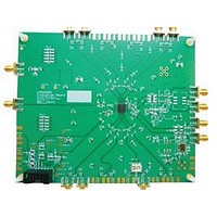
General Description The LMK03200 Evaluation Board simplifies evaluation of the LMK03200 Precision Clock Conditioner with Integrated VCO. The package consists of an ...
Page 4
Read first, Basic Operation First install the CodeLoader 4 software. This can be downloaded from: http://www.national.com/timing/software/ For basic operation… 1. Connect a ...
Page 5
Read first, Basic Operation (Continued) 3. Connect… • PC directly to the evaluation board with the LPT to uWire cable, plugging the ...
Page 6
Read first, Basic Operation (Continued) 4. Start CodeLoader 4. Figure 3 - Starting CodeLoader 4 5. Select the USB or LPT Communication ...
Page 7
Read first, Basic Operation (Continued) 7. Enable output to be measured, any of CLKout(0-7) or EN_Fout from either Clock Outputs or Bits/Pins ...
Page 8
Engaging 0-Delay Mode To engage 0-Delay mode a two step programming sequence is followed as described in the datasheet. Following this document’s ...
Page 9
FB_MUX setting = CLKout6 and CLKout6 is not enabled, the following warning will display: FB_MUX setting = FBCLKin and CLKout5 and 6 ...
Page 10
Board Information OSCin By default the board is configured to use the on-board crystal oscillator also possible to use the ...
Page 11
... SYNC* pin is low, divided outputs will not oscillate but the bypassed outputs will continue to oscillate. • For both loop filters, a helper silkscreen is offset from the loop filters to help identify the components according to National Semiconductor’s traditional reference designators associated with loop filters. • The silk screen Fin/Fin* designates the FBCLKin/FBCLKin* port. ...
Page 12
Recommended Equipment Power Supply The Power Supply should be a low noise power supply. Phase Noise / Spectrum Analyzer For measuring phase ...
Page 13
Phase Noise Figure 8 - Fout at 1244.16 MHz Figure 9 – LVDS output CLKout2 at 155.52 MHz ...
Page 14
Figure 10 – LVPECL output CLKout4 at 155.52 MHz Reference Oscillator Phase Noise note: The performance of the on-board crystal can be ...
Page 15
Delays These delay measurements illustrate how skew errors due to different length traces may be tuned out. The delay may be adjusted in steps of ~150 ps. Figure 11 – Delays Figure ...
Page 16
CodeLoader Settings Figure 13 - Port Setup Tab & Selecting a Default Mode The Port Setup tab tells CodeLoader what signals are ...
Page 17
The Bits/Pins tab shows some of the internal registers which are not accessible from any of the o ther visual tabs like ...
Page 18
The Registers tab shows the raw bits which will be programmed when device is loaded b clicking K eyboard Controls Load Device ...
Page 19
The PLL tab shows a conventional PLL diagram along with the VCO Divider important to realize that the total effective ...
Page 20
Appendix A: Impact of Reference on Phase Noise Inside the loop bandwidth of a PLL the phase noise is set by the ...
Page 21
Appendix B: Schematics LMK03200 - Main Board LMK03200 - Main Board.sch ...
Page 22
Vcc Vin R5 0 ohm SMA C3 Open ...
Page 23
Vcc Vcc CLKout0 R85 R86 Open Open C84 CLKout0 SMA CLKout0 CLKout1 0.1 uF R93 Open C88 CLKout0* SMA CLKout0* CLKout1* 0.1 ...
Page 24
Appendix C: Bill of Materials Part Manufacturer Capacitors 100 pF Kem 12 nF Kemet 0.1 uF Kemet 0.1 uF Kemet 1 uF ...
Page 25
Other 3.3 V zener Comchip ADT2-1T Minicircuits Frame Printed Circuits Corp HEADER_2X5(POLARIZED) FCI Ele National LMK03200 Semiconductor Crystek 3391-19.440 Crystek SMA Johnson ...
Page 26
Open - Open - Open - Open - Open - Open - Open - Open - Open - Open - BOM Version ...
Page 27
Appendix D: Build Diagram ...
Page 28
Bottom Build Diagram (Mirrored ...