LMK03200EVAL National Semiconductor, LMK03200EVAL Datasheet - Page 11
LMK03200EVAL
Manufacturer Part Number
LMK03200EVAL
Description
BOARD EVALUATION LMK03200
Manufacturer
National Semiconductor
Specifications of LMK03200EVAL
Main Purpose
Timing, Clock Conditioner
Embedded
No
Utilized Ic / Part
LMK03200
Primary Attributes
3 LVDS & 5 LVPECL Outputs, Integrated PLL & VCO
Secondary Attributes
3.15 V ~ 3.45 V Supply
Silicon Manufacturer
National
Silicon Core Number
LMK03200
Kit Application Type
Clock & Timing
Application Sub Type
Precision Clock Conditioner
Kit Contents
Board, Cable
Lead Free Status / RoHS Status
Lead free / RoHS Compliant


Features of the board
Other Important Notes
•
•
•
•
•
•
•
•
•
•
•
•
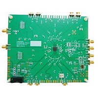
Either one of two loop filters can be selected by shorting either R69 or R72. More info
about the loop filter can be found in the General Description. The second loop filter on
the bottom of the board is unpopulated for customer use.
Test points for each of the uWire lines are scattered in the lower left corner of the board
and include: GOE_TP, DATAuWire, CLKuWire, LEuWire, SYNC_TP, and LD_TP.
Ground is located on the unstuffed 10 pin header on the left side of the board.
Ground is located on the GND_tp2 in the upper left corner of the board and GND_tp1
located to the right of the Vcc SMA connector.
Ground is located on the bottom side of the board on each pad of the unstuffed 10 pin
header GND_J2.
Vcc is located on the unstuffed 10 pin header on the upper left side of the board.
Vcc is located on VccPlane test point located to the right of the Vcc SMA.
Vcc is located on the bottom side of the board on each pad of the unstuffed 10 pin
header VCC_J2
When changing the OSCin frequency, the OSCin frequency register needs to match.
Toggle the SYNC* pin to synchronize the clock outputs when in divided mode. If the
SYNC* pin is low, divided outputs will not oscillate but the bypassed outputs will continue
to oscillate.
For both loop filters, a helper silkscreen is offset from the loop filters to help identify the
components according to National Semiconductor’s traditional reference designators
associated with loop filters.
The silk screen Fin/Fin* designates the FBCLKin/FBCLKin* port.
L M K 0 3 2 0 0
E V A L U A T I O N
11
B O A R D
O P E R A T I N G
I N S T R U C T I O N S
Related parts for LMK03200EVAL
Image
Part Number
Description
Manufacturer
Datasheet
Request
R

Part Number:
Description:
Precision 0-delay Clock Conditioner With Integrated Vco
Manufacturer:
National Semiconductor Corporation
Datasheet:

Part Number:
Description:
National Semiconductor [8-Bit D/A Converter]
Manufacturer:
National Semiconductor
Datasheet:
Part Number:
Description:
National Semiconductor [Media Coprocessor]
Manufacturer:
National Semiconductor
Datasheet:
Part Number:
Description:
Digitally Controlled Tone and Volume Circuit with Stereo Audio Power Amplifier, Microphone Preamp Stage and National 3D Sound
Manufacturer:
National Semiconductor
Datasheet:
Part Number:
Description:
Digitally Controlled Tone and Volume Circuit with Stereo Audio Power Amplifier, Microphone Preamp Stage and National 3D Sound
Manufacturer:
National Semiconductor
Datasheet:
Part Number:
Description:
AC97 Rev 2 Codec with Sample Rate Conversion and National 3D Sound
Manufacturer:
National Semiconductor
Part Number:
Description:
Manufacturer:
National Semiconductor
Datasheet:
Part Number:
Description:
Manufacturer:
National Semiconductor
Datasheet:
Part Number:
Description:
General Purpose, Low Voltage, Low Power, Rail-to-Rail Output Operational Amplifiers
Manufacturer:
National Semiconductor
Datasheet:
Part Number:
Description:
8-bit 20 MSPS flash A/D converter.
Manufacturer:
National Semiconductor
Datasheet:
Part Number:
Description:
Low Noise Quad Operational Amplifier
Manufacturer:
National Semiconductor
Datasheet:
Part Number:
Description:
Quad Differential Line Receivers
Manufacturer:
National Semiconductor
Datasheet:
Part Number:
Description:
Quad High Speed Trapezoidal? Bus Transceiver
Manufacturer:
National Semiconductor
Datasheet:
Part Number:
Description:
Dual Line Receiver
Manufacturer:
National Semiconductor
Datasheet: