MCP3421EV Microchip Technology, MCP3421EV Datasheet - Page 10
MCP3421EV
Manufacturer Part Number
MCP3421EV
Description
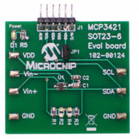
BOARD EVAL FOR MCP3421 SOT23-6
Manufacturer
Microchip Technology
Specifications of MCP3421EV
Design Resources
MCP3421EV Gerber Files
Number Of Adc's
1
Number Of Bits
18
Sampling Rate (per Second)
4
Data Interface
Serial
Inputs Per Adc
1 Single Ended
Input Range
±2.5 V
Voltage Supply Source
Single Supply
Operating Temperature
-40°C ~ 125°C
Utilized Ic / Part
MCP3421
Silicon Manufacturer
Microchip
Application Sub Type
ADC
Kit Application Type
Data Converter
Silicon Core Number
MCP3421
Kit Contents
Board
Rohs Compliant
Yes
Lead Free Status / RoHS Status
Not applicable / Not applicable
Available stocks
Company
Part Number
Manufacturer
Quantity
Price
Company:

Part Number:
MCP3421EV
Manufacturer:
Microchip Technology
Quantity:
135


MCP3421
3.4
SDA is the serial data pin of the I
pin is used for input and output data. In read mode, the
conversion result is read from the SDA pin (output). In
write mode, the device configuration bits are written
(input) though the SDA pin. The SDA pin is an open-
drain N-channel driver. Therefore, it needs a pull-up
resistor from the V
start and stop conditions, the data on the SDA pin must
be stable during the high period of the clock. The high
or low state of the SDA pin can only change when the
clock signal on the SCL pin is low. Refer to Section 5.3
“I
Serial Interface communication.
FIGURE 3-1:
DS22003E-page 10
2
C Serial Communications” for more details of I
Legend:
V
IN
Serial Data Pin (SDA)
+, V
V
C
R
PIN
R
IN
V
SS
V = Signal Source
SS
T
- = Analog Input Pin
DD
= Source Impedance
= Input Pin Capacitance
= Threshold Voltage
V
Equivalent Analog Input Circuit.
line to the SDA pin. Except for
IN
+,V
IN
-
2
C interface. The SDA
4 pF
C
PIN
D
D
1
2
V
DD
V
V
T
T
= 0.6V
= 0.6V
2
C
V
SS
I
C
LEAKAGE
SAMPLE
D
Typical range of the pull-up resistor value for SCL and
SDA is from 5 kΩ to 10 kΩ for standard (100 kHz) and
fast (400 kHz) modes, and less than 1 kΩ for high
speed mode (3.4 MHz). The High-Speed mode is not
recommended for V
1
I
(~ ±1 nA)
, D
LEAKAGE
SS = Sampling Switch
R
S
2
=
= Leakage Current at Analog Pin
= Sampling Switch Resistor
= Sample Capacitance
ESD Protection Diode
SS
Sampling
Switch
DD
less than 2.7V.
© 2009 Microchip Technology Inc.
R
S
C
(3.2 pF)
SAMPLE
Related parts for MCP3421EV
Image
Part Number
Description
Manufacturer
Datasheet
Request
R

Part Number:
Description:
Manufacturer:
Microchip Technology Inc.
Datasheet:
Part Number:
Description:
Manufacturer:
Microchip Technology Inc.
Datasheet:
Part Number:
Description:
Manufacturer:
Microchip Technology Inc.
Datasheet:
Part Number:
Description:
Manufacturer:
Microchip Technology Inc.
Datasheet:
Part Number:
Description:
Manufacturer:
Microchip Technology Inc.
Datasheet:
Part Number:
Description:
Manufacturer:
Microchip Technology Inc.
Datasheet:
Part Number:
Description:
Manufacturer:
Microchip Technology Inc.
Datasheet:
Part Number:
Description:
Manufacturer:
Microchip Technology Inc.
Datasheet: