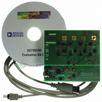
EVAL-AD7991EBZ Analog Devices Inc, EVAL-AD7991EBZ Datasheet
EVAL-AD7991EBZ
Specifications of EVAL-AD7991EBZ


Related parts for EVAL-AD7991EBZ


EVAL-AD7991EBZ Summary of contents
Page 1
FEATURES 12-/10-/8-bit ADCs with fast conversion time: 1 μs typical 4 analog input channels/3 analog input channels with reference input Specified for Sequencer operation Temperature range: −40°C to +125° C-compatible ...
Page 2
AD7991/AD7995/AD7999 TABLE OF CONTENTS Features .............................................................................................. 1 Applications....................................................................................... 1 Functional Block Diagram .............................................................. 1 General Description ......................................................................... 1 Product Highlights ........................................................................... 1 Revision History ............................................................................... 2 Specifications..................................................................................... 3 AD7991 .......................................................................................... 3 AD7995 .......................................................................................... 5 AD7999 .......................................................................................... ...
Page 3
SPECIFICATIONS 1 AD7991 The temperature range of the Y version is −40°C to +125°C. Unless otherwise noted, V and MIN MAX Table 2. Parameter DYNAMIC PERFORMANCE 2, 3 Signal-to-Noise and Distortion (SINAD) Signal-to-Noise ...
Page 4
AD7991/AD7995/AD7999 Parameter LOGIC INPUTS (SDA, SCL) Input High Voltage, V INH Input Low Voltage, V INL Input Leakage Current Input Capacitance Input Hysteresis, V HYST LOGIC OUTPUTS (OPEN DRAIN) Output Low Voltage Floating-State ...
Page 5
AD7995 The temperature range for the Y version is −40°C to +125°C. Unless otherwise noted, V and MIN MAX Table 3. A Version Parameter Min Typ DYNAMIC PERFORMANCE Signal-to-Noise ...
Page 6
AD7991/AD7995/AD7999 A Version Parameter Min Typ LOGIC INPUTS (SDA, SCL) Input High Voltage INH DD Input Low Voltage, V INL Input Leakage Current Input Capacitance Input Hysteresis ...
Page 7
AD7999 The temperature range for the Y version is −40°C to +125°C. Unless otherwise noted, V and MIN MAX Table 4. A Version Parameter Min Typ DYNAMIC PERFORMANCE Signal-to-Noise ...
Page 8
AD7991/AD7995/AD7999 A Version Parameter Min Typ LOGIC INPUTS (SDA, SCL) Input High Voltage INH DD Input Low Voltage, V INL Input Leakage Current Input Capacitance Input Hysteresis ...
Page 9
I C TIMING SPECIFICATIONS Guaranteed by initial characterization. All values were measured with the input filtering enabled. C with t and t measured between 0 Table 5. Parameter Conditions 1 f Standard mode SCL Fast ...
Page 10
AD7991/AD7995/AD7999 Parameter Conditions t Standard mode 10 Fast mode High speed mode C = 100 pF maximum 400 pF maximum B t Standard mode 11 Fast mode High speed mode C = 100 pF maximum B C ...
Page 11
ABSOLUTE MAXIMUM RATINGS T = 25°C, unless otherwise noted. A Table 6. Parameter V to GND DD Analog Input Voltage to GND Reference Input Voltage to GND Digital Input Voltage to GND Digital Output Voltage to GND Input Current to ...
Page 12
AD7991/AD7995/AD7999 PIN CONFIGURATION AND FUNCTION DESCRIPTIONS Table 7. Pin Function Descriptions Pin No. Mnemonic Description 1 SCL Digital Input. Serial bus clock. External pull-up resistor required. 2 SDA Digital I/O. Serial bus bidirectional data. Open-drain output. External pull-up resistor required. ...
Page 13
TYPICAL PERFORMANCE CHARACTERISTICS 1.0 0.8 0.6 0.4 0.2 0 –0.2 –0.4 –0.6 –0.8 –1.0 0 500 1000 1500 2000 2500 CODE Figure 4. DNL Error 2 2. REF Without Clock Stretching 1.0 ...
Page 14
AD7991/AD7995/AD7999 1.0 0.8 0.6 0.4 0.2 0 –0.2 –0.4 –0 2.5V –0.8 REF f = 1.7MHz SCL –1.0 0 500 1000 1500 2000 2500 CODE Figure 10. DNL Error ...
Page 15
POINT FFT f = 95kSPS S f –20 SCL f IN SNR = 71.77dB SINAD = 71.45dB –40 THD = –82.43dB SFDR = –95.02dB –60 –80 –100 –120 FREQUENCY (kHz) ...
Page 16
AD7991/AD7995/AD7999 TERMINOLOGY Signal-to-Noise and Distortion (SINAD) Ratio The measured ratio of signal-to-noise and distortion at the output of the ADC. The signal is the rms amplitude of the fundamental. Noise is the sum of the nonfundamental signals excluding dc, up ...
Page 17
THEORY OF OPERATION The AD7991/AD7995/AD7999 are low power, 12-/10-/8-bit, single-supply, 4-channel ADCs. Each part can be operated from a single 2. 5.5 V supply. The AD7991/AD7995/AD7999 provide the user with a 4-channel multiplexer, an on-chip track-and-hold, an ADC, ...
Page 18
AD7991/AD7995/AD7999 TYPICAL CONNECTION DIAGRAM Figure 22 shows the typical connection diagram for the AD7991/AD7995/AD7999. The reference voltage can be taken from the supply voltage However, the AD7991/AD7995/AD7999 can be configured 3-channel device with the ...
Page 19
For ac applications, removing high frequency components from the analog input signal is recommended by use band- pass filter on the relevant analog input pin. In applications where harmonic distortion and signal-to-noise ratio are critical, the analog ...
Page 20
AD7991/AD7995/AD7999 INTERNAL REGISTER STRUCTURE CONFIGURATION REGISTER The configuration register is an 8-bit write-only register that is used to set the operating modes of the AD7991/AD7995/AD7999. The bit functions are outlined in Table 10. A single-byte write is necessary when writing ...
Page 21
SAMPLE DELAY AND BIT TRIAL DELAY recommended that bus activity occur while a conversion is taking place (see Figure 27 and the Placing the AD7991/AD7995/AD7999 into High Speed Mode section). However, if this is ...
Page 22
AD7991/AD7995/AD7999 SERIAL INTERFACE Control of the AD7991/AD7995/AD7999 is accomplished via 2 the I C-compatible serial bus. The AD7991/AD7995/AD7999 is connected to this bus as a slave device under the control of a master device, such as the processor. SERIAL BUS ...
Page 23
WRITING TO THE AD7991/AD7995/AD7999 By default, each part operates in read-only mode and all four chan- nels are selected as enabled in the configuration register. To write to the AD7991/AD7995/AD7999 configuration register, the user must first address the device. 1 ...
Page 24
AD7991/AD7995/AD7999 READING FROM THE AD7991/AD7995/AD7999 Reading data from the conversion result register is a 2-byte operation, as shown in Figure 25. Therefore, a read operation always involves two bytes. After the AD7991/AD7995/AD7999 have received a read address, any number of ...
Page 25
PLACING THE AD7991/AD7995/AD7999 INTO HIGH SPEED MODE High speed mode communication commences after the master addresses all devices connected to the bus with the master code, 00001XXX, to indicate that a high speed mode transfer is to begin. No device ...
Page 26
AD7991/AD7995/AD7999 MODE OF OPERATION The AD7991/AD7995/AD7999 powers up in shutdown mode. After the master addresses the AD7991/AD7995/AD7999 with 2 the correct I C address, the ADC acknowledges the address. In response, the AD7991/AD7995/AD7999 power up. During this wake up time, ...
Page 27
... AD7995YRJZ-0RL −40°C to +125°C AD7995YRJZ-0500RL7 −40°C to +125°C AD7995ARJZ-0RL −40°C to +125°C AD7999YRJZ-1RL −40°C to +125°C AD7999YRJZ-1500RL7 −40°C to +125°C AD7999ARJZ-1RL −40°C to +125°C EVAL-AD7991EBZ EVAL-AD7995EBZ RoHS Compliant Part. 3.00 2.90 2. 3.00 2.80 2 ...
Page 28
AD7991/AD7995/AD7999 NOTES ©2007–2010 Analog Devices, Inc. All rights reserved. Trademarks and registered trademarks are the property of their respective owners. D06461-0-10/10(B) Rev Page ...