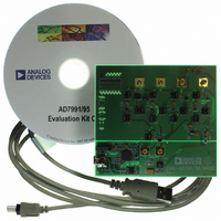
EVAL-AD7991EBZ Analog Devices Inc, EVAL-AD7991EBZ Datasheet - Page 20
EVAL-AD7991EBZ
Manufacturer Part Number
EVAL-AD7991EBZ
Description
BOARD EVAL FOR AD7991
Manufacturer
Analog Devices Inc
Specifications of EVAL-AD7991EBZ
Number Of Adc's
1
Number Of Bits
12
Sampling Rate (per Second)
1M
Data Interface
Serial
Inputs Per Adc
4 Single Ended
Input Range
0 ~ Vdd
Power (typ) @ Conditions
4.4mW @ 5.5 V, 3.4MHz
Voltage Supply Source
Single Supply
Operating Temperature
-40°C ~ 125°C
Utilized Ic / Part
AD7991
Silicon Manufacturer
Analog Devices
Application Sub Type
ADC
Kit Application Type
Data Converter
Silicon Core Number
AD7991
Kit Contents
Board
Rohs Compliant
Yes
Lead Free Status / RoHS Status
Lead free / RoHS Compliant


AD7991/AD7995/AD7999
INTERNAL REGISTER STRUCTURE
CONFIGURATION REGISTER
The configuration register is an 8-bit write-only register that is used to set the operating modes of the AD7991/AD7995/AD7999. The bit
functions are outlined in Table 10. A single-byte write is necessary when writing to the configuration register. D7 is the MSB. When the
master writes to the AD7991/AD7995/AD7999, the first byte is written to the configuration register.
Table 9. Configuration Register Bit Map and Default Settings at Power-Up
D7
CH3
1
Table 10. Bit Function Descriptions
Bit
D7 to D4
D3
D2
D1
D0
Table 11. Channel Selection
D7
0
0
0
0
0
0
0
0
1
1
1
1
1
1
1
1
1
The AD7991/AD7995/AD7999 converts on the selected channel in the sequence in ascending order, starting with the lowest channel in the sequence.
CH2
D6
1
D6
0
0
0
0
1
1
1
1
0
0
0
0
1
1
1
1
Mnemonic
REF_SEL
FLTR
Bit trial delay
Sample delay
CH3 to CH0
D5
CH1
1
D5
0
0
1
1
0
0
1
1
0
0
1
1
0
0
1
1
Comment
These four channel address bits select the analog input channel(s) to be converted. If a channel address bit
(Bit D7 to Bit D4) is set to 1, a channel is selected for conversion. If more than one channel bit is set to 1, the
AD7991/AD7995/AD7999 sequence through the selected channels, starting with the lowest channel. All
unused channels should be set to 0. Table 11 shows how these four channel address bits are decoded. Prior
to the device initiating a conversion, the channel(s) must be selected in the configuration register.
This bit allows the user to select the supply voltage as the reference or choose to use an external reference. If
this bit is 0, the supply is used as the reference, and the device acts as a 4-channel input part. If this bit is set
to 1, an external reference must be used and applied to the V
input part.
The value written to this bit of the control register determines whether the filtering on SDA and SCL is
enabled or bypassed. If this bit is set to 0, the filtering is enabled; if it set to 1, the filtering is bypassed.
See the Sample Delay and Bit Trial Delay section.
See the Sample Delay and Bit Trial Delay section.
D4
CH0
1
0
1
0
1
0
1
0
1
0
1
0
1
0
1
0
1
D4
D3
REF_SEL
0
Analog Input Channel
No channel selected
Convert on V
Convert on V
Sequence between V
Convert on V
Sequence between V
Sequence between V
Sequence among V
Convert on V
Sequence between V
Sequence between V
Sequence among V
Sequence between V
Sequence among V
Sequence among V
Sequence among V
D2
FLTR
0
Rev. B | Page 20 of 28
IN0
IN1
IN2
IN3
IN0
IN0
IN0
IN1
IN0
IN0
IN0
IN1
IN0
IN1
IN2
, V
, V
, V
, V
, V
1
and V
and V
and V
IN1
and V
and V
IN1
and V
IN2
IN2
IN1
, and V
, and V
, and V
, and V
, V
D1
Bit trial delay
0
IN2
IN1
IN2
IN2
IN3
IN3
IN3
, and V
IN2
IN3
IN3
IN3
IN3
IN3
/V
REF
pin, and the device acts as a 3-channel
D0
Sample delay
0
Related parts for EVAL-AD7991EBZ
Image
Part Number
Description
Manufacturer
Datasheet
Request
R


Part Number:
Description:
BOARD EVAL FOR SI270X-A
Manufacturer:
Silicon Laboratories Inc
Datasheet:

Part Number:
Description:
BUCK CONV REF DESIGN KIT IP1201
Manufacturer:
International Rectifier
Datasheet:
Part Number:
Description:
BOARD DEMO SYNC DUAL BUCK CNVTER
Manufacturer:
International Rectifier
Datasheet:
Part Number:
Description:
BOARD DEMO SYNC BUCK CONVETER
Manufacturer:
International Rectifier
Datasheet:

Part Number:
Description:
EVALBOARD/EB Omnidirectional microphone - Analog
Manufacturer:
Analog Devices
Datasheet:
Part Number:
Description:
EVALBOARD/EB Omnidirectional microphone - Analog
Manufacturer:
Analog Devices
Datasheet:


Part Number:
Description:
BOARD EVAL LED DRIVER LT3756
Manufacturer:
Linear Technology
Datasheet:

Part Number:
Description:
BOARD EVAL FOR AD7741/7742
Manufacturer:
Analog Devices Inc
Datasheet:

Part Number:
Description:
±1.7g Dual-Axis IMEMS Accelerometer Evaluation Board
Manufacturer:
Analog Devices Inc
Datasheet:

Part Number:
Description:
IC MULTIPLIER ANALOG 8-SOIC T/R
Manufacturer:
Analog Devices Inc
Datasheet:

Part Number:
Description:
IC ANALOG MULTIPLIER 8-DIP
Manufacturer:
Analog Devices Inc
Datasheet:
Part Number:
Description:
IC ANALOG MULTIPLIER 8-SOIC
Manufacturer:
Analog Devices Inc
Datasheet:
Part Number:
Description:
IC ANALOG MULTIPLIER 8-DIP
Manufacturer:
Analog Devices Inc
Datasheet: