EVAL-AD7991EBZ Analog Devices Inc, EVAL-AD7991EBZ Datasheet - Page 17
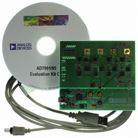
EVAL-AD7991EBZ
Manufacturer Part Number
EVAL-AD7991EBZ
Description
BOARD EVAL FOR AD7991
Manufacturer
Analog Devices Inc
Specifications of EVAL-AD7991EBZ
Number Of Adc's
1
Number Of Bits
12
Sampling Rate (per Second)
1M
Data Interface
Serial
Inputs Per Adc
4 Single Ended
Input Range
0 ~ Vdd
Power (typ) @ Conditions
4.4mW @ 5.5 V, 3.4MHz
Voltage Supply Source
Single Supply
Operating Temperature
-40°C ~ 125°C
Utilized Ic / Part
AD7991
Silicon Manufacturer
Analog Devices
Application Sub Type
ADC
Kit Application Type
Data Converter
Silicon Core Number
AD7991
Kit Contents
Board
Rohs Compliant
Yes
Lead Free Status / RoHS Status
Lead free / RoHS Compliant


THEORY OF OPERATION
The AD7991/AD7995/AD7999 are low power, 12-/10-/8-bit,
single-supply, 4-channel ADCs. Each part can be operated from
a single 2.35 V to 5.5 V supply.
The AD7991/AD7995/AD7999 provide the user with a 4-channel
multiplexer, an on-chip track-and-hold, an ADC, and an I
compatible serial interface, all housed in an 8-lead SOT-23 package
that offers the user considerable space-saving advantages over
alternative solutions.
The AD7991/AD7995/AD7999 normally remains in a power-
down state while not converting. Therefore, when supplies are
first applied, the part is in a power-down state. Power-up is initiated
prior to a conversion, and the device returns to the power-down
state upon completion of the conversion. This automatic power-
down feature allows the device to save power between conversions.
This means any read or write operations across the I
can occur while the device is in power-down.
CONVERTER OPERATION
The AD7991/AD7995/AD7999 are successive approximation
ADCs built around a capacitive DAC. Figure 18 and Figure 19
show simplified schematics of the ADC during its acquisition
and conversion phases, respectively. Figure 18 shows the ADC
during its acquisition phase: SW2 is closed, SW1 is in Position A,
the comparator is held in a balanced condition, and the sampling
capacitor acquires the signal on V
analog input needs to settle the analog input signal to within
one LSB in 0.6 μs, which is equivalent to the duration of the
power-up and acquisition time.
AGND
V
IN
A
SW1
B
Figure 18. ADC Acquisition Phase
SW2
IN
. The source driving the
COMPARATOR
CAPACITIVE
CONTROL
2
LOGIC
C interface
DAC
2
C-
Rev. B | Page 17 of 28
When the ADC starts a conversion, as shown in Figure 19, SW2
opens and SW1 moves to Position B, causing the comparator to
become unbalanced. The input is disconnected when the con-
version begins. The control logic and the capacitive DAC are used
to add and subtract fixed amounts of charge from the sampling
capacitor to bring the comparator back into a balanced condition.
When the comparator is rebalanced, the conversion is complete.
The control logic generates the ADC output code. Figure 20 shows
the ADC transfer function.
ADC Transfer Function
The output coding of the AD7991/AD7995/AD7999 is straight
binary. The designed code transitions occur at successive integer
LSB values (that is, 1 LSB, 2 LSB, and so on). The LSB size for
the AD7991/AD7995/AD7999 is V
V
characteristics for the AD7991/AD7995/AD7999.
AGND
REF
V
IN
/256, respectively. Figure 20 shows the ideal transfer
Figure 20. AD7991/AD7995/AD7999 Transfer Characteristics
SW1
A
111 ... 111
111 ... 110
111 ... 000
011 ... 111
000 ... 010
000 ... 001
000 ... 000
B
Figure 19. ADC Conversion Phase
AGND + 1 LSB
AD7991/AD7995/AD7999
SW2
ANALOG INPUT
AD7991 1 LSB = REF
AD7995 1 LSB = REF
AD7999 1 LSB = REF
0V TO REF
REF
COMPARATOR
/4096, V
+REF
IN
IN
– 1 LSB
REF
IN
IN
IN
/1024, and
CAPACITIVE
/4096
/1024
/256
CONTROL
LOGIC
DAC
Related parts for EVAL-AD7991EBZ
Image
Part Number
Description
Manufacturer
Datasheet
Request
R


Part Number:
Description:
BOARD EVAL FOR SI270X-A
Manufacturer:
Silicon Laboratories Inc
Datasheet:

Part Number:
Description:
BUCK CONV REF DESIGN KIT IP1201
Manufacturer:
International Rectifier
Datasheet:
Part Number:
Description:
BOARD DEMO SYNC DUAL BUCK CNVTER
Manufacturer:
International Rectifier
Datasheet:
Part Number:
Description:
BOARD DEMO SYNC BUCK CONVETER
Manufacturer:
International Rectifier
Datasheet:

Part Number:
Description:
EVALBOARD/EB Omnidirectional microphone - Analog
Manufacturer:
Analog Devices
Datasheet:
Part Number:
Description:
EVALBOARD/EB Omnidirectional microphone - Analog
Manufacturer:
Analog Devices
Datasheet:


Part Number:
Description:
BOARD EVAL LED DRIVER LT3756
Manufacturer:
Linear Technology
Datasheet:

Part Number:
Description:
BOARD EVAL FOR AD7741/7742
Manufacturer:
Analog Devices Inc
Datasheet:

Part Number:
Description:
±1.7g Dual-Axis IMEMS Accelerometer Evaluation Board
Manufacturer:
Analog Devices Inc
Datasheet:

Part Number:
Description:
IC MULTIPLIER ANALOG 8-SOIC T/R
Manufacturer:
Analog Devices Inc
Datasheet:

Part Number:
Description:
IC ANALOG MULTIPLIER 8-DIP
Manufacturer:
Analog Devices Inc
Datasheet:
Part Number:
Description:
IC ANALOG MULTIPLIER 8-SOIC
Manufacturer:
Analog Devices Inc
Datasheet:
Part Number:
Description:
IC ANALOG MULTIPLIER 8-DIP
Manufacturer:
Analog Devices Inc
Datasheet: