KDC5514EVALZ Intersil, KDC5514EVALZ Datasheet - Page 23
KDC5514EVALZ
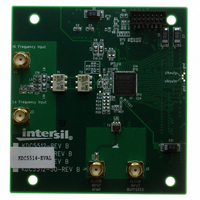
Manufacturer Part Number
KDC5514EVALZ
Description
DAUGHTER CARD FOR KAD5514
Manufacturer
Intersil
Series
FemtoCharge™r
Datasheets
1.KAD5514P-25Q72.pdf
(34 pages)
2.KMB-001LEVALZ.pdf
(7 pages)
3.KDC5514EVALZ.pdf
(9 pages)
Specifications of KDC5514EVALZ
Number Of Adc's
1
Number Of Bits
14
Sampling Rate (per Second)
250M
Data Interface
Parallel
Inputs Per Adc
1 Differential
Input Range
1.47 Vpp
Power (typ) @ Conditions
429mW @ 250MSPS
Voltage Supply Source
Single Supply
Operating Temperature
-40°C ~ 85°C
Utilized Ic / Part
KAD5514P-25, KMB001 Motherboard
For Use With
KMB001LEVAL - MOTHERBOARD FOR LVDS ADC CARD
Lead Free Status / RoHS Status
Lead free / RoHS Compliant
Other names
KDC5514EVAL
KDC5514EVAL
KDC5514EVAL
Available stocks
Company
Part Number
Manufacturer
Quantity
Price
Company:

Part Number:
KDC5514EVALZ
Manufacturer:
Intersil
Quantity:
5


SPI Physical Interface
The serial clock pin (SCLK) provides synchronization for the
data transfer. By default, all data is presented on the serial
data input/output (SDIO) pin in three-wire mode. The state of
the SDIO pin is set automatically in the communication
protocol (described in the following). A dedicated serial data
output pin (SDO) can be activated by setting 0x00[7] high to
allow operation in four-wire mode.
The SPI port operates in a half duplex master/slave
configuration, with the KAD5514P functioning as a slave.
Multiple slave devices can interface to a single master in
three-wire mode only, since the SDO output of an
unaddressed device is asserted in four-wire mode.
The chip-select bar (CSB) pin determines when a slave
device is being addressed. Multiple slave devices can be
written to concurrently, but only one slave device can be
read from at a given time (again, only in three-wire mode). If
multiple slave devices are selected for reading at the same
time, the results will be indeterminate.
The communication protocol begins with an
instruction/address phase. The first rising SCLK edge
following a high to low transition on CSB determines the
beginning of the two-byte instruction/address command,
SCLK must be static low before the CSB transition. Data can
be presented in MSB-first order or LSB-first order. The
default is MSB-first, but this can be changed by setting
0x00[6] high. Figures 35 and 36 show the appropriate bit
ordering for the MSB-first and LSB-first modes, respectively.
CSB
SCLK
SDIO
t
S
R/W
CSB
SCLK
SDIO
SDO
t
DSW
23
W1
t
S
R/W W1 W0 A12 A11 A10 A9
t
DSW
W0
A12
t
DHW
t
A11
DHW
t
WRITING A READ COMMAND
HI
t
HI
A10
FIGURE 37. WRITE TIMING
FIGURE 38. READ TIMING
t
LO
t
LO
A9
t
KAD5514P
t
CLK
CLK
SPI WRITE
A2
SPI READ
A8
A1
t
DVR
A7
A0
In MSB-first mode the address is incremented for multi-byte
transfers, while in LSB-first mode it’s decremented.
In the default mode the MSB is R/W, which determines if the
data is to be read (active high) or written. The next two bits,
W1 and W0, determine the number of data bytes to be read
or written (see Table 6). The lower 13 bits contain the first
address for the data transfer. This relationship is illustrated in
Figure 37, and timing values are given in the “Switching
Specifications” on page 8.
After the instruction/address bytes have been read, the
appropriate number of data bytes are written to or read from
the ADC (based on the R/W bit status). The data transfer will
continue as long as CSB remains low and SCLK is active.
Stalling of the CSB pin is allowed at any byte boundary
(instruction/address or data) if the number of bytes being
transferred is three or less. For transfers of four bytes or
more, CSB is allowed stall in the middle of the
instruction/address bytes or before the first data byte. If CSB
transitions to a high state after that point the state machine
will reset and terminate the data transfer.
READING DATA
D7
D7
D6
D5
D3
(4 WIRE MODE)
TABLE 6. BYTE TRANSFER SELECTION
[W1:W0]
D3 D2
D4
(3 WIRE MODE)
00
01
10
11
D2
D3
t
DHR
D1 D0
D1
t
H
D0
D2
D1
D0
BYTES TRANSFERRED
t
H
4 or more
1
2
3
September 10, 2009
FN6804.2
Related parts for KDC5514EVALZ
Image
Part Number
Description
Manufacturer
Datasheet
Request
R

Part Number:
Description:
DAUGHTER CARD FOR KAD5514
Manufacturer:
Intersil
Datasheet:

Part Number:
Description:
Intersil Corporation [CMOS Serial Controller Interface]
Manufacturer:
Intersil Corporation
Datasheet:
Part Number:
Description:
Manufacturer:
Intersil Corporation
Datasheet:
Part Number:
Description:
357-036-542-201 CARDEDGE 36POS DL .156 BLK LOPRO
Manufacturer:
Intersil Corporation
Datasheet:
Part Number:
Description:
1024-Word x 4-Bit LSI Static RAM
Manufacturer:
Intersil Corporation
Datasheet:
Part Number:
Description:
General Purpose NPN Transistor Arrays FN341.4
Manufacturer:
Intersil Corporation
Datasheet:
Part Number:
Description:
CMOS 16-Bit Microprocessor
Manufacturer:
Intersil Corporation
Datasheet:
Part Number:
Description:
Manufacturer:
Intersil Corporation
Datasheet:
Part Number:
Description:
Manufacturer:
Intersil Corporation
Datasheet:
Part Number:
Description:
Manufacturer:
Intersil Corporation
Datasheet:
Part Number:
Description:
Manufacturer:
Intersil Corporation
Datasheet:
Part Number:
Description:
CMOS 6-Bit Latch and Decoder Memory Interfaces
Manufacturer:
Intersil Corporation
Datasheet:
Part Number:
Description:
CA3046General Purpose NPN Transistor Arrays
Manufacturer:
Intersil Corporation
Datasheet:
Part Number:
Description:
Manufacturer:
Intersil Corporation
Datasheet:
Part Number:
Description:
TR909 DLC/FLC SLIC with Low Power Standby
Manufacturer:
Intersil Corporation
Datasheet: