EVAL-AD7730EBZ Analog Devices Inc, EVAL-AD7730EBZ Datasheet

BOARD EVAL FOR AD7730

EVAL-AD7730EBZ

Manufacturer Part Number
EVAL-AD7730EBZ
Description
BOARD EVAL FOR AD7730
Manufacturer
Analog Devices Inc
Datasheet

Specifications of EVAL-AD7730EBZ

Number Of Adc's
1
Number Of Bits
24
Sampling Rate (per Second)
1.2k
Data Interface
Serial
Inputs Per Adc
2 Differential
Input Range
±80 mV
Power (typ) @ Conditions
125mW @ 1.2kSPS
Voltage Supply Source
Analog and Digital
Operating Temperature
-40°C ~ 85°C
Utilized Ic / Part
AD7730
Lead Free Status / RoHS Status
Lead free / RoHS Compliant
Other names
EVAL-AD7730EB
EVAL-AD7730EB
a
INTRODUCTION
This Application Note describes the evaluation board for the
AD7730, Transducer ADC. The AD7730 is a complete analog
front-end for weigh-scale and pressure measurement
applications. The device accepts low-level signals directly from a
transducer and outputs a serial digital word. The part features
two buffered differential programmable gain analog inputs as
well as a differential reference input. An on-chip 6-bit DAC
allows the removal of TARE voltages. Clock signals for
synchronizing ac excitation of the bridge are also provided. Full
data on the AD7730 is available in the AD7730 data sheet
available from Analog Devices and should be consulted in
conjunction with this Application Note when using the
Evaluation Board.
Included on the evaluation board, along with the AD7730, are
an AD780, a +2.5 V ultra high precision bandgap reference, a
4.9152MHz crystal and digital buffers to buffer signals to and
from the edge connectors.
REV. A
Information furnished by Analog Devices is believed to be accurate and
reliable. However, no responsibility is assumed by Analog Devices for its
use, nor for any infringements of patents or other rights of third parties
which may result from its use. No license is granted by implication or
otherwise under any patent or patent rights of Analog Devices.
FEATURES
Operates from a Single +5V Supply
On-Board Reference and Digital Buffers
Various Linking Options
Direct Hook-Up to Printer Port of PC
PC Software for Control and Data Analysis
AIN2(+)/D1
AIN2(-)/D0
AIN1(+)
AIN1(-)
AV DD
ACX
ACX
AGND
DV DD
REFERENCE
FUNCTIONAL BLOCK DIAGRAM
AD780
DGND
REF IN
AD7730
ADC
AV DD
Interfacing to this board is provided either through a 36-Way
Centronics Connector or through a 9-way D-type connector.
External sockets are provided for the analog inputs, an external
reference input option and an external master clock option.
OPERATING THE AD7730 EVALUATION BOARD
Power Supplies
The evaluation board has four power supply input pins: AV
AGND, DV
AV
board must be +5V. This AV
AD780 reference. To run the board from a single +5V supply,
simply connect the AV
Both AGND and DGND inputs are provided on the board.
AGND connects to the AD7730 AGND pin and also connects
to the GND pin of the AD780. DGND connects to the DGND
pin of the AD7730 and to the GND of the digital chips on the
board. The AGND and DGND planes are connected at the
AD7730. Therefore, it is recommended not to connect AGND
and DGND elsewhere in the system to avoid ground loop
problems. When using a single supply for both AV
only one ground connection should be made to the board. This
connection should be made to the board's AGND input
terminal.
Both supplies are decoupled to their respective ground plane
with 10 F tantalum and 0.1 F ceramic disc capacitors.
One Technology Way, P.O. Box 9106, Norwood. MA 02062-9106, U.S.A.
Tel: 617/329-4700
MCLK IN
DD
9-WAY D-TYPE CONNECTOR
of +5V. Therefore, the AV
BUFFERS
DD
and DGND. The AD7730 is specified with an
Evaluation Board for
DD
CENTRONICS
CONNECTOR
and DV
36-WAY
EVAL-AD7730EB
DD
Transducer ADC
voltage is also used to power the
DD
DD
voltage supplied to the
inputs together.
Fax: 617/326-8703
DD
and DV
DD
DD
,
,

Related parts for EVAL-AD7730EBZ

EVAL-AD7730EBZ Summary of contents

Page 1

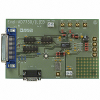
... Analog Devices and should be consulted in conjunction with this Application Note when using the Evaluation Board. Included on the evaluation board, along with the AD7730, are an AD780, a +2.5 V ultra high precision bandgap reference, a 4.9152MHz crystal and digital buffers to buffer signals to and from the edge connectors ...

Page 2

... EVAL-AD7730EB Link Options There are a number of link options on the evaluation board which should be set for the required operating setup before using the board. The functions of these link options are described in detail below. Link No. Function LK1 This option selects the master clock option for the AD7730. The master clock source comes from the on-board crystal or from an external clock source via SKT11 ...

Page 3

... LK11 IN SKT4 connected to AIN1(-). EVALUATION BOARD INTERFACING Interfacing to the evaluation board is either via a 9-way D-Type connector, SKT1 36-way Centronics connector, SKT2. The pinout for the SKT1 connector is given in Figure 1 and its corresponding pin designations are given in Table II. The pinout for this SKT2 connector is shown in Figure 2 and its pin designations are given in Table III ...

Page 4

... NC No Connect. These pins are not connected on the evaluation board. 19-30 DGND Ground reference point for digital circuitry. Connects to the DGND plane on the evaluation board. 31- Connect. These pins are not connected on the evaluation board. Figure 3. SKT2 Pin Configuration Table III. SKT2 Pin Designations – ...

Page 5

... SOCKETS There are eleven sockets on the AD7730 evaluation board. The function of these sockets is outlined in Table IV. Table IV. Socket Functions Socket Function SKT1 9-Way D-Type Connector which can be used for digital interfacing to the evaluation board. SKT2 36-Way Centronics Connector which can be used for digital interfacing to the evaluation board. This ...

Page 6

... AD7730 software. Select Printer Port This button allows the user to select the printer port to which the AD7730 evaluation is connected. About This provides details of the software revision. Figure 4. Main Screen –6– ...

Page 7

... REV. A Figure 5. Program Screen Figure 6. Mode Register Screen –7– EVAL-AD7730EB ...

Page 8

... A 2 MCLK IN LK1 IC1 AD7730 C16 MCLK OUT 3 XTAL1 ACX 17 ACX 16 LK3 REF IN(-) LK5 A REF IN(+) 14 STANDBY C8 0 IC2 LK2 AD780 B 4 Figure 7. Evaluation Board Circuit Diagram –8– SKT ACK SLCT GND DOUT DGND CS SCLK SYNC RDY R6 10k DGND RESET ...

Related keywords