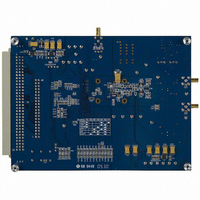
EVAL-AD7678CB Analog Devices Inc, EVAL-AD7678CB Datasheet - Page 17

EVAL-AD7678CB
Manufacturer Part Number
EVAL-AD7678CB
Description
BOARD EVALUATION FOR AD7678
Manufacturer
Analog Devices Inc
Series
PulSAR®r
Specifications of EVAL-AD7678CB
Number Of Adc's
1
Number Of Bits
18
Sampling Rate (per Second)
100k
Data Interface
Serial, Parallel
Inputs Per Adc
1 Differential
Input Range
±VREF
Power (typ) @ Conditions
31mW @ 100kSPS
Voltage Supply Source
Analog and Digital
Operating Temperature
-40°C ~ 85°C
Utilized Ic / Part
AD7678
Lead Free Status / RoHS Status
Contains lead / RoHS non-compliant
TYPICAL CONNECTION DIAGRAM
Figure 21 shows a typical connection diagram for the AD7678.
Different circuitry shown on this diagram is optional and is
discussed later in this data sheet.
Analog Inputs
Figure 22 shows a simplified analog input section of the
AD7678. The diodes shown in Figure 22 provide ESD protec-
tion for the inputs. Care must be taken to ensure that the analog
input signal never exceeds the absolute ratings on these inputs.
This will cause these diodes to become forward-biased and start
conducting current. These diodes can handle a forward-biased
current of 120 mA max. This condition could eventually occur
when the input buffer’s U1 or U2 supplies are different from
AVDD. In such a case, an input buffer with a short-circuit
current limitation can be used to protect the part.
This analog input structure is a true differential structure. By
using these differential inputs, signals common to both inputs
are rejected as shown in Figure 23, which represents typical
CMRR over frequency.
80
75
70
65
60
55
50
IN+
IN–
1
Figure 23. Analog Input CMRR vs. Frequency
AGND
Figure 22. Simplified Analog Input
AVDD
10
FREQUECY (kHz)
100
R+ = 3k
R– = 3k
C
C
1000
S
S
03084-0-028
03084-0-029
10000
Rev. A | Page 17 of 28
During the acquisition phase for ac signals, the AD7678 behaves
like a 1-pole RC filter consisting of the equivalent resistance,
R+, R–, and C
lumped components made up of a serial resistor and the on
resistance of the switches. C
consists of the ADC sampling capacitor. This 1-pole filter with a
–3 dB cutoff frequency of 900 kHz typ reduces any undesirable
aliasing effect and limits the noise coming from the inputs.
Because the input impedance of the AD7678 is very high, the
part can be driven directly by a low impedance source without
gain error.
Driver Amplifier Choice
Although the AD7678 is easy to drive, the driver amplifier
needs to meet the following requirements:
The driver amplifier and the AD7678 analog input circuit
have to be able to settle for a full-scale step of the capacitor
array at an 18-bit level (0.0004%). In the amplifier’s data
sheet, settling at 0.1% or 0.01% is more commonly
specified. This could differ significantly from the settling
time at an 18-bit level and, therefore, should be verified
prior to driver selection. The tiny op amp AD8021, which
combines ultralow noise and high gain-bandwidth, meets
this settling time requirement.
The noise generated by the driver amplifier needs to be
kept as low as possible in order to preserve the SNR and
transition noise performance of the AD7678. The noise
coming from the driver is filtered by the AD7678 analog
input circuit 1-pole low-pass filter made by R+, R–, and C
The SNR degradation due to the amplifier is
where:
f
(0.9 MHz).
N is the noise factor of the amplifiers (1 if in buffer
configuration).
e
nV/Hz.
For instance, for a driver with an equivalent input noise of
6 nV/Hz (e.g., AD8610) configured as a buffer, thus with
a noise gain of +1, the SNR degrades by only 0.65 dB.
The driver needs to have a THD performance suitable to
that of the AD7678.
–3dB
N
is the equivalent input noise voltage of each op amp in
is the –3 dB input bandwidth in MHz of the AD7678
SNR
S
. Resistors R+ and R– are typically 3 k and are
LOSS
20
log
S
is typically 60 pF and mainly
625
f
–
25
3dB
(
Ne
N
2 )
AD7678
S
.


