EVAL-AD7725CBZ Analog Devices Inc, EVAL-AD7725CBZ Datasheet - Page 13
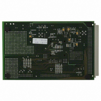
EVAL-AD7725CBZ
Manufacturer Part Number
EVAL-AD7725CBZ
Description
BOARD EVALUATION FOR AD7725
Manufacturer
Analog Devices Inc
Datasheet
1.AD7725BSZ.pdf
(28 pages)
Specifications of EVAL-AD7725CBZ
Number Of Adc's
1
Number Of Bits
16
Sampling Rate (per Second)
900k
Data Interface
Serial, Parallel
Inputs Per Adc
1 Differential
Input Range
±VREF
Power (typ) @ Conditions
615mW @ 900kSPS
Voltage Supply Source
Analog and Digital
Operating Temperature
-40°C ~ 85°C
Utilized Ic / Part
AD7725
Lead Free Status / RoHS Status
Lead free / RoHS Compliant


TERMINOLOGY
Integral Nonlinearity (INL)
This is the maximum deviation of any code from a straight line
passing through the endpoints of the transfer function. The
endpoints of the transfer function are zero scale (not to be
confused with bipolar zero), a point 0.5 LSB below the first
code transition (100 . . . 00 to 100 . . . 01 in bipolar mode,
000 . . . 00 to 000 . . . 01 in unipolar mode) and full scale, a
point 0.5 LSB above the last code transition (011 . . . 10 to
011 . . . 11 in bipolar mode, 111 . . . 10 to 111 . . . 11 in
unipolar mode). The error is expressed in LSBs.
Differential Nonlinearity (DNL)
This is the difference between the measured and the ideal
1 LSB change between two adjacent codes in the ADC.
Unipolar Offset Error
Unipolar offset error is the deviation of the first code transition
from the ideal V
operating in the unipolar mode.
Bipolar Offset Error
This is the deviation of the midscale transition code
(111 . . . 11 to 000 . . . 00) from the ideal V
which is (V
Gain Error
The first code transition should occur at an analog value
0.5 LSB above negative full scale. The last code transition
should occur for an analog value 1.5 LSB below the nominal
full scale. Gain error is the deviation of the actual difference
between first and last code transitions and the ideal difference
between first and last code transitions.
Signal-to-Noise Ratio (SNR)
SNR is the measured signal-to-noise ratio at the output of the
ADC. The signal is the rms magnitude of the fundamental.
Noise is the rms sum of all of the nonfundamental signals up to
half the output data rate (f
evaluated by applying a low noise, low distortion sine wave
signal to the input pins. By generating a Fast Fourier Trans-
form (FFT) plot, the SNR data can then be obtained from the
output spectrum.
REV. A
IN
(–) – 0.5 LSB) when operating in the bipolar mode.
IN
(+) voltage, which is (V
O
/2), excluding dc. The ADC is
IN
(–) + 0.5 LSB) when
IN
(+) voltage,
–13–
Total Harmonic Distortion (THD)
THD is the ratio of the rms sum of the harmonics to the rms
value of the fundamental. THD is defined as
where V
V
sixth harmonics.
Spurious Free Dynamic Range (SFDR)
Defined as the difference, in dB, between the peak spurious or
harmonic component in the ADC output spectrum (up to
f
Normally, the value of this specification will be determined by
the largest harmonic in the output spectrum of the FFT. For
input signals whose second harmonics occur in the stop band
region of the digital filter, the spur in the noise floor limits
the SFDR.
Settling Time and Group Delay
The settling time of a digital filter is dependent on the amount
of decimation employed and the number of filter taps used in
the filter design and is calculated as follows:
The settling time for each filter stage should be calculated
separately and then added to get the total filter settling time.
Group delay is half the settling time.
O
4
/2 and excluding dc) and the rms value of the fundamental.
, V
5
, and V
settling time
1
is the rms amplitude of the fundamental and V
THD =
6
are the rms amplitudes of the second through
20 log
=
data input rate
V
2
2
1
+
V
3
2
+
V
V
×
1
4
2
number of taps
+
V
5
2
AD7725
+
V
6
2
2
, V
3
,
Related parts for EVAL-AD7725CBZ
Image
Part Number
Description
Manufacturer
Datasheet
Request
R


Part Number:
Description:
BOARD EVAL FOR SI270X-A
Manufacturer:
Silicon Laboratories Inc
Datasheet:

Part Number:
Description:
BUCK CONV REF DESIGN KIT IP1201
Manufacturer:
International Rectifier
Datasheet:
Part Number:
Description:
BOARD DEMO SYNC DUAL BUCK CNVTER
Manufacturer:
International Rectifier
Datasheet:
Part Number:
Description:
BOARD DEMO SYNC BUCK CONVETER
Manufacturer:
International Rectifier
Datasheet:

Part Number:
Description:
EVALBOARD/EB Omnidirectional microphone - Analog
Manufacturer:
Analog Devices
Datasheet:
Part Number:
Description:
EVALBOARD/EB Omnidirectional microphone - Analog
Manufacturer:
Analog Devices
Datasheet:


Part Number:
Description:
BOARD EVAL LED DRIVER LT3756
Manufacturer:
Linear Technology
Datasheet:

Part Number:
Description:
BOARD EVAL FOR AD7741/7742
Manufacturer:
Analog Devices Inc
Datasheet:

Part Number:
Description:
±1.7g Dual-Axis IMEMS Accelerometer Evaluation Board
Manufacturer:
Analog Devices Inc
Datasheet:

Part Number:
Description:
IC MULTIPLIER ANALOG 8-SOIC T/R
Manufacturer:
Analog Devices Inc
Datasheet:

Part Number:
Description:
IC ANALOG MULTIPLIER 8-DIP
Manufacturer:
Analog Devices Inc
Datasheet:
Part Number:
Description:
IC ANALOG MULTIPLIER 8-SOIC
Manufacturer:
Analog Devices Inc
Datasheet:
Part Number:
Description:
IC ANALOG MULTIPLIER 8-DIP
Manufacturer:
Analog Devices Inc
Datasheet: