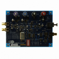
CDB5340 Cirrus Logic Inc, CDB5340 Datasheet - Page 3

CDB5340
Manufacturer Part Number
CDB5340
Description
BOARD EVAL FOR CS5340 STEREO ADC
Manufacturer
Cirrus Logic Inc
Specifications of CDB5340
Number Of Adc's
1
Number Of Bits
24
Sampling Rate (per Second)
192k
Data Interface
Serial
Inputs Per Adc
2 Single
Power (typ) @ Conditions
180mW @ 5 V
Voltage Supply Source
Analog and Digital
Operating Temperature
-10°C ~ 70°C
Utilized Ic / Part
CS5340
Product
Audio Modules
Lead Free Status / RoHS Status
Contains lead / RoHS non-compliant
Lead Free Status / RoHS Status
Lead free / RoHS Compliant, Contains lead / RoHS non-compliant
Other names
598-1544
1. CDB5340 SYSTEM OVERVIEW
The CDB5340 evaluation board is an excellent means of quickly evaluating the CS5340. The
CS8406 digital audio interface transmitter provides an easy interface to digital audio signal ana-
lyzers including the majority of digital audio test equipment.
The CDB5340 schematic has been partitioned into 5 schematics shown in
Figure
Notice that the system diagram also includes the interconnections between the
partitioned schematics.
2. CS8406 DIGITAL AUDIO TRANSMITTER
The system generates and encodes standard S/PDIF data using a CS8406 Digital Audio Trans-
mitter (see
The CS8406 supports both Left Justified and I
S2. A description of the CS8406 is included in the CS8406 datasheet.
3. INPUT/OUTPUT FOR CLOCKS AND DATA
The evaluation board has been designed to allow interfacing to external systems via the 10-pin
header, J11. The schematic for the clock/data input/output is shown in
The CDB5340 allows some flexibility as to the generation of the clocks. When the CS5340 and
CS8406 are in slave mode, the SCLK and LRCK must be provided via the header, J11. MCLK
can be generated from the on-board oscillator, Y1 or provided via the header, J11 as determined
by the DIP switch, S2. The on-board oscillator is socketed to allow other frequency oscillators to
be used. Please note that the on-board oscillator must be removed if an external MCLK is pro-
vided through header J11.
4. POWER SUPPLY CIRCUITRY
Power is supplied to the evaluation board by four binding posts (VA/VD, VL, GND, +5V),
see
to the VL pin of the CS5340 and to the level shifter circuits. The +5V input supplies power to the
digital circuitry and the input amplifiers.
5. GROUNDING AND POWER SUPPLY DECOUPLING
The CS5340 requires careful attention to power supply and grounding arrangements to optimize
performance.
itors are located as close to the CS5340 as possible. Extensive use of ground plane fill in the
evaluation board yields large reductions in radiated noise.
6. ANALOG INPUT FILTER
The CDB5340 implements a single-ended analog input buffer, as shown in
there is no attenuation or gain associated with the input buffer.
DS601DB1
Figure
6. Each partitioned schematic is represented in the system diagram shown in
Figure
6. The VA/VD input supplies the VA and VD pins of the CS5340. VL supplies power
Figure 3
5). The outputs of the CS8406 are RS422 compatible differential line drivers.
details the power distribution used on this board. The decoupling capac-
2
S data formats, as determined by the DIP switch,
Figure
Figure
4.
Figure 2
CDB5340
2. Note that
Figure
through
1.
3


