CDB5340 Cirrus Logic Inc, CDB5340 Datasheet - Page 4
CDB5340
Manufacturer Part Number
CDB5340
Description
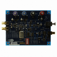
BOARD EVAL FOR CS5340 STEREO ADC
Manufacturer
Cirrus Logic Inc
Specifications of CDB5340
Number Of Adc's
1
Number Of Bits
24
Sampling Rate (per Second)
192k
Data Interface
Serial
Inputs Per Adc
2 Single
Power (typ) @ Conditions
180mW @ 5 V
Voltage Supply Source
Analog and Digital
Operating Temperature
-10°C ~ 70°C
Utilized Ic / Part
CS5340
Product
Audio Modules
Lead Free Status / RoHS Status
Contains lead / RoHS non-compliant
Lead Free Status / RoHS Status
Lead free / RoHS Compliant, Contains lead / RoHS non-compliant
Other names
598-1544


4
J5
J6
J11
S1
S2
* denotes default factory settings
VA/VD
VL
GND
+5V
AINL
AINR
Optical Output
Coax Output
JUMPER/SWITCH
CONNECTOR
VA/VD Power Source
VL Power Source
Input/Output for
clocks/data
Reset for the CDB5340
CDB5340 Configuration
Input
Input
Input
Input
Input
Input
Output
Output
INPUT/OUTPUT
PURPOSE
Table 2. CDB5340 Jumper and Switch Settings
Table 1. System Connections
Ground connection from power supply
Analog input left channel
Analog input right channel
+3.3V to +5V power for the CS5340
+2.5V to +5V power for the CS5340
+ 5 Volt power
Digital audio output
Digital audio output
ADJ
*+3.3V
+5V
ADJ
*+3.3V
+5V
-
-
M1/M0
SCLK/LRCK Open
MCLK
8406
DIF
POSITION
Open
*Closed
*Closed
Open
*Closed
Open
*Closed
Open
*Closed
SIGNAL PRESENT
Power from the Binding Post (J1)
Power from the +3.3V Regulator
Power from the +5V Supply
Power from the Binding Post (J2)
Power from the +3.3V Regulator
Power from the +5V Supply
-
-
Hi
Low
Header J11 is an input for clocks.
Header J11 is an output for clocks.
Header J11 is an input for MCLK.
Header J11 is an output for MCLK.
CS8406 in Master mode
CS8406 in Slave mode
Digital interface format set to I
Digital interface format set to
Left Justified
FUNCTION SELECTED
CDB5340
DS601DB1
2
S
Related parts for CDB5340
Image
Part Number
Description
Manufacturer
Datasheet
Request
R

Part Number:
Description:
Development Kit
Manufacturer:
Cirrus Logic Inc
Datasheet:
Part Number:
Description:
Development Kit
Manufacturer:
Cirrus Logic Inc
Datasheet:


Part Number:
Description:
High-efficiency PFC + Fluorescent Lamp Driver Reference Design
Manufacturer:
Cirrus Logic Inc
Datasheet:
Part Number:
Description:
Development Kit
Manufacturer:
Cirrus Logic Inc
Datasheet:
Part Number:
Description:
Development Kit
Manufacturer:
Cirrus Logic Inc
Datasheet:

Part Number:
Description:
Development Kit
Manufacturer:
Cirrus Logic Inc
Datasheet:
Part Number:
Description:
Development Kit
Manufacturer:
Cirrus Logic Inc
Datasheet:
Part Number:
Description:
Development Kit
Manufacturer:
Cirrus Logic Inc
Datasheet:
Part Number:
Description:
Development Kit
Manufacturer:
Cirrus Logic Inc
Datasheet:

Part Number:
Description:
EVALUATION BOARD FOR CS8427
Manufacturer:
Cirrus Logic Inc
Datasheet:

Part Number:
Description:
BOARD EVAL FOR CS8416 RCVR
Manufacturer:
Cirrus Logic Inc
Datasheet:

Part Number:
Description:
EVALUATION BOARD FOR CS8420
Manufacturer:
Cirrus Logic Inc
Datasheet:

Part Number:
Description:
KIT DEVELOPMENT EP9315 ARM9
Manufacturer:
Cirrus Logic Inc
Datasheet:

Part Number:
Description:
KIT DEVELOPMENT EP9302 ARM9
Manufacturer:
Cirrus Logic Inc
Datasheet: