DEMOTS4956J STMicroelectronics, DEMOTS4956J Datasheet - Page 4
DEMOTS4956J
Manufacturer Part Number
DEMOTS4956J
Description
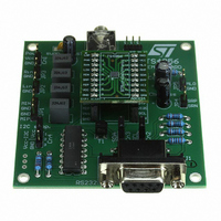
BOARD DEMO TS4956EIJT/EIKJT
Manufacturer
STMicroelectronics
Specifications of DEMOTS4956J
Amplifier Type
Class AB
Output Type
1-Channel (Mono) with Mono and Stereo Headphones
Max Output Power X Channels @ Load
1W x 1 @ 8 Ohm; 43mW x 2 @ 32 Ohm
Voltage - Supply
2.7 V ~ 5.5 V
Operating Temperature
-40°C ~ 85°C
Board Type
Fully Populated
Utilized Ic / Part
TS4956
Description/function
Audio Amplifiers
Operating Supply Voltage
2.7 V to 5.5 V
Product
Audio Modules
Lead Free Status / RoHS Status
Lead free / RoHS Compliant
For Use With/related Products
TS4956
Other names
497-6381
DEMOTS4956J
DEMOTS4956J
Available stocks
Company
Part Number
Manufacturer
Quantity
Price


Absolute maximum ratings and operating conditions
1
4/55
Absolute maximum ratings and operating conditions
Table 1.
1. All voltage values are measured with respect to the ground pin.
2. The magnitude of input signal must never exceed V
3. Device is protected in case of over temperature by a thermal shutdown activated at 150°C.
4. Exceeding the power derating curves during a long period may involve abnormal operating conditions.
5. Human body model, 100 pF discharged through a 1.5 kΩ resistor, into pin to V
Table 2.
1. For proper functionality of I2C bus, V
2. With heat sink surface 120 mm
Table 3.
1. Must be less than or equal to the power supply voltage V
Latch-up
Symbol
Symbol
Symbol
I
V
and clock wires and cause dysfunction of I
2
T
P
ESD
F
R
R
V
CV
T
CC
V
V
R
C
V
oper
I
SCL
V
T
diss
thja
thja
CC
stg
IN
ILl
IH
ol
L
L
i
j
(1)
CC
Supply voltage
Input voltage
Operating free air temperature range
Storage temperature
Maximum junction temperature
Thermal resistance junction to ambient
Power dissipation
Susceptibility - human body model
Susceptibility - machine model
Lead temperature (soldering, 10sec)
Supply voltage
Load resistor
Load capacitor
Flip-chip thermal resistance junction to ambient
Latch-up immunity
I2C supply voltage
Maximum low level input voltage on pins SDA, SCL
Minimum high level input voltage
Maximum input current (pins SDA, SCL), 0.4 V < V
SCL maximum clock frequency
Max low level output voltage, SDA pin, I
Absolute maximum ratings
Operating conditions
I
2
Speaker/BTL output (modes 1,2,7)
Headphone, MLO output (modes 3,4,5,6,)
R
R
3,4,5,6)
R
C electrical characteristics
L
L
L
= 8 Ω to 100 Ω (speaker/BTL output - modes 1,2,7)
= 16 Ω to 100 Ω (headphone, MLO output - modes
> 100 Ω
(2)
(1)
2
.
(1)
Parameter
CC
Parameter
pins must not be grounded. ESD protection diodes ground data
Parameter
2
C bus in this condition.
(5)
CC
+ 0.3 V / GND - 0.3 V
(3)
sink
CC
of the device.
= 3 mA
in
< 4.5 V
Internally limited
G
-65 to +150
-40 to + 85
ND
CC
Value
150
200
150
200
260
to V
6
2
device
0.3 I2CVCC
0.7 I2CVCC
2.7 to 5.5 V
2.7 to 5.5 V
CC
Value
Value
400
90
0.4
10
500
400
100
≥
≥
(4)
16
8
(2)
TS4956
°C/W
Unit
°C/W
mA
Unit
Unit
°C
°C
°C
kV
°C
kHz
V
V
V
µA
pF
V
Ω
V
V
V
V
Related parts for DEMOTS4956J
Image
Part Number
Description
Manufacturer
Datasheet
Request
R

Part Number:
Description:
Manufacturer:
STMicroelectronics
Datasheet:

Part Number:
Description:
DEMO BOARD FOR HMC6042/HMC1041Z
Manufacturer:
Honeywell Microelectronics & Precision Sensors

Part Number:
Description:
DEMO BOARD FOR HMC1042L/HMC1041Z
Manufacturer:
Honeywell Microelectronics & Precision Sensors
Datasheet:

Part Number:
Description:
KIT DEMO 4 SENSOR CHAN RS232
Manufacturer:
VTI Technologies
Datasheet:


Part Number:
Description:
DEMO: DC Power Supply, 32 Volts, 3 Amps
Manufacturer:
Tektronix
Part Number:
Description:
DEMO: Programmable DC Power Supply, 32 Volts, 3 Amps
Manufacturer:
Tektronix
Part Number:
Description:
STMicroelectronics [RIPPLE-CARRY BINARY COUNTER/DIVIDERS]
Manufacturer:
STMicroelectronics
Datasheet:
Part Number:
Description:
STMicroelectronics [LIQUID-CRYSTAL DISPLAY DRIVERS]
Manufacturer:
STMicroelectronics
Datasheet:

Part Number:
Description:
BOARD EVAL FOR MEMS SENSORS
Manufacturer:
STMicroelectronics
Datasheet:
Part Number:
Description:
NPN TRANSISTOR POWER MODULE
Manufacturer:
STMicroelectronics
Datasheet:
Part Number:
Description:
TURBOSWITCH ULTRA-FAST HIGH VOLTAGE DIODE
Manufacturer:
STMicroelectronics
Datasheet: