DEMOTS4956J STMicroelectronics, DEMOTS4956J Datasheet - Page 7
DEMOTS4956J
Manufacturer Part Number
DEMOTS4956J
Description
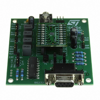
BOARD DEMO TS4956EIJT/EIKJT
Manufacturer
STMicroelectronics
Specifications of DEMOTS4956J
Amplifier Type
Class AB
Output Type
1-Channel (Mono) with Mono and Stereo Headphones
Max Output Power X Channels @ Load
1W x 1 @ 8 Ohm; 43mW x 2 @ 32 Ohm
Voltage - Supply
2.7 V ~ 5.5 V
Operating Temperature
-40°C ~ 85°C
Board Type
Fully Populated
Utilized Ic / Part
TS4956
Description/function
Audio Amplifiers
Operating Supply Voltage
2.7 V to 5.5 V
Product
Audio Modules
Lead Free Status / RoHS Status
Lead free / RoHS Compliant
For Use With/related Products
TS4956
Other names
497-6381
DEMOTS4956J
DEMOTS4956J
Available stocks
Company
Part Number
Manufacturer
Quantity
Price


TS4956
2.1
2.1.1
I
The TS4956 uses a serial bus, which conforms to the I
powered when it is connected to the I
clock and data.
The clock and data lines are bidirectional (open-collector) with an external chip pull-up
resistor (typically 10 kΩ). The maximum clock frequency in fast-mode specified by the I
standard is 400 kHz, and this frequency is supported by the TS4956. In this application, the
TS4956 is always the slave device and the controlling MCU is the master device.
The I2CVCC pin determines the power supply of the TS4956’s I
connected to this pin must be equal to or less than the TS4956 power supply voltage V
The minimum value of the I2CVCC voltage is 2.7 V.
When the I2CVCC pin is connected to an I
via the I
When the I2CVCC pin is connected to the ground, the TS4956 is in total standby mode, with
an ultra-low standby current on the order of a few nanoamperes. In this condition the
TS4956 cannot receive I
In both cases, pins SDA and SCL must respect logic HI or logic LOW thresholds (not
floating) presented in
Table 5
Table 5.
I²C operation description
The host MCU can write into the TS4946 control register to control the TS4956 and read
from the control register to get the current configuration of the TS4956. The TS4956 is
addressed by a single byte consisting of a 7-bit slave address and an R/W bit. The TS4956
control register address is $5Dh.
Table 6.
In order to write data into the TS4956 control register, after the "start" message the MCU
must send the following data:
●
●
All bytes are sent with the MSB bit first. The transfer of written data ends with a "stop"
message. When transmitting several bits of data, the data can be written without having to
repeat the "start" message or address byte with the slave address.
SDA
SCL
I2CVCC
2
C interface
A6
send byte with the I²C 7-bit slave address and with the R/W bit set low.
send the data (control register setting).
1
summarizes the pin descriptions for the I²C bus interface.
2
C bus.
I²C bus interface: pin descriptions
First byte after the START message for addressing the device
A5
0
Pin
Table 3 on page
2
C commands from the I
A4
1
2
A3
C bus), to control the chip’s functions via two wires:
4, in order for the circuit to function properly.
1
2
C voltage, the TS4956 is ready to communicate
Serial data pin
Clock input pin
I
2
C interface power supply
2
A2
C bus.
1
2
C protocol (the TS4956 must be
Functional description
Typical application schematic
A1
0
2
C interface. The voltage
A0
1
Rw
X
2
CC
C
7/55
.
Related parts for DEMOTS4956J
Image
Part Number
Description
Manufacturer
Datasheet
Request
R

Part Number:
Description:
Manufacturer:
STMicroelectronics
Datasheet:

Part Number:
Description:
DEMO BOARD FOR HMC6042/HMC1041Z
Manufacturer:
Honeywell Microelectronics & Precision Sensors

Part Number:
Description:
DEMO BOARD FOR HMC1042L/HMC1041Z
Manufacturer:
Honeywell Microelectronics & Precision Sensors
Datasheet:

Part Number:
Description:
KIT DEMO 4 SENSOR CHAN RS232
Manufacturer:
VTI Technologies
Datasheet:


Part Number:
Description:
DEMO: DC Power Supply, 32 Volts, 3 Amps
Manufacturer:
Tektronix
Part Number:
Description:
DEMO: Programmable DC Power Supply, 32 Volts, 3 Amps
Manufacturer:
Tektronix
Part Number:
Description:
STMicroelectronics [RIPPLE-CARRY BINARY COUNTER/DIVIDERS]
Manufacturer:
STMicroelectronics
Datasheet:
Part Number:
Description:
STMicroelectronics [LIQUID-CRYSTAL DISPLAY DRIVERS]
Manufacturer:
STMicroelectronics
Datasheet:

Part Number:
Description:
BOARD EVAL FOR MEMS SENSORS
Manufacturer:
STMicroelectronics
Datasheet:
Part Number:
Description:
NPN TRANSISTOR POWER MODULE
Manufacturer:
STMicroelectronics
Datasheet:
Part Number:
Description:
TURBOSWITCH ULTRA-FAST HIGH VOLTAGE DIODE
Manufacturer:
STMicroelectronics
Datasheet: