NCP2809AEVB ON Semiconductor, NCP2809AEVB Datasheet - Page 15
NCP2809AEVB
Manufacturer Part Number
NCP2809AEVB
Description
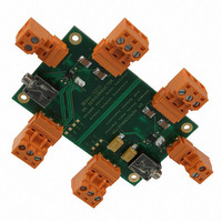
EVAL BOARD FOR NCP2809A
Manufacturer
ON Semiconductor
Series
NOCAP™r
Specifications of NCP2809AEVB
Design Resources
NCP2809AEVB BOM NCP2809AEVB Gerber Files NCP2809AEVB Schematic
Amplifier Type
Class AB
Output Type
Headphones, 2-Channel (Stereo)
Max Output Power X Channels @ Load
135mW x 2 @ 16 Ohm
Voltage - Supply
2.2 V ~ 5.5 V
Board Type
Fully Populated
Utilized Ic / Part
NCP2809
Lead Free Status / RoHS Status
Lead free / RoHS Compliant
Operating Temperature
-
Lead Free Status / Rohs Status
Lead free / RoHS Compliant
For Use With/related Products
NCP2809A
Other names
NCP2809AEVBOS
Available stocks
Company
Part Number
Manufacturer
Quantity
Price
Company:

Part Number:
NCP2809AEVB
Manufacturer:
ON Semiconductor
Quantity:
2


The dissipated power by the device is
At a given power supply voltage, the maximum power
dissipated is:
application, each load with the same output power will give
the same dissipated power. Thus the total lost power for the
device is:
And in this case, the maximum power dissipated will be:
In single ended operation, the efficiency is:
output coupling capacitors, then the current provided by
the battery for one output is as following:
•
•
So, the total power delivered by the battery to the device is:
The power in the load is P
The dissipated power by the device is
V
I
O
p
Of course, if the device is used in a typical stereo
If the application requires a NOCAP scheme without
V
consider a sine wave signal with a period T and a peak
voltage V
R
(t)
/R
o
L
L
(t) is the AC voltage seen by the load. Here we
is the load.
P TOT + V p
P TOT +
I p avg + 1 p
O
.
P D +
T/2
P D + P TOT * P OUT
P D +
P Dmax +
P Dmax +
2V p .V o
p.R L
P OUT +
R L
V o
h +
I p avg
V o
R L
p
0
OUT
V o
R L
p.V O
2p 2 .R L
p 2 .R L
2V P
2V P
V P 2
T
V P 2
p
V O 2
sin(t)dt +
2R L
V P
p
* V O
* V O
2
p.R L
2V o
TIME
http://onsemi.com
15
At a given power supply voltage, the maximum power
dissipated happens when V
application, each load with the same output power will give
the same dissipated power. Thus the total lost power for the
device is:
And in this case, the maximum power dissipated will be:
In NOCAP operation, the efficiency is:
Gain−Setting Selection
a closed−loop gain of 0db for the NCP2809A and an
external gain setting with the NCP2809B. In order to
optimize device and system performance, NCP2809 needs
to be used in low gain configurations. It minimizes THD+N
values and maximizes the signal−to−noise ratio, and the
amplifier can still be used without running into the
bandwidth limitations.
Adjustable gain is available on NCP2809B.
NCP2809 Amplifier External Components
Input Capacitor Selection (C
the amplifier input terminal. This capacitor creates a
high−pass filter with the internal (A version with 20 kW) or
external (B version) resistor. Its cut−off frequency is given
by:
in low frequencies without severe attenuation. However a
large input coupling capacitor requires more time to reach
its quiescent DC voltage (V
turn−on pops.
many applications (in case of R
Of course, if the device is used in a typical stereo
With NCP2809 Audio Amplifier family, you can select
NCP2809A can be used when a 0 dB gain is required.
The input coupling capacitor blocks the DC voltage at
The size of the capacitor must be large enough to couple
An input capacitor value of 100 nF performs well in
P D +
f c +
P D + P TOT * P OUT
P D +
P Dmax +
P Dmax +
V o
R L
2 * p * R in * C in
h +
V o
R L
O
p.V O
4V P
= Vp/2.
in
4V P
0.19V P 2
0.38V P 2
P
1
)
p
/2) and can increase the
2V P
in
R L
R L
p
= 20 kW).
* V O
* V O
2
(eq. 1)
Related parts for NCP2809AEVB
Image
Part Number
Description
Manufacturer
Datasheet
Request
R

Part Number:
Description:
ON Semiconductor [VOLTAGE REGULATOR]
Manufacturer:
ON Semiconductor
Datasheet:
Part Number:
Description:
357-036-542-201 CARDEDGE 36POS DL .156 BLK LOPRO
Manufacturer:
ON Semiconductor
Datasheet:
Part Number:
Description:
357-036-542-201 CARDEDGE 36POS DL .156 BLK LOPRO
Manufacturer:
ON Semiconductor
Datasheet:
Part Number:
Description:
357-036-542-201 CARDEDGE 36POS DL .156 BLK LOPRO
Manufacturer:
ON Semiconductor
Datasheet:
Part Number:
Description:
357-036-542-201 CARDEDGE 36POS DL .156 BLK LOPRO
Manufacturer:
ON Semiconductor
Datasheet:
Part Number:
Description:
357-036-542-201 CARDEDGE 36POS DL .156 BLK LOPRO
Manufacturer:
ON Semiconductor
Datasheet:
Part Number:
Description:
357-036-542-201 CARDEDGE 36POS DL .156 BLK LOPRO
Manufacturer:
ON Semiconductor
Datasheet:
Part Number:
Description:
357-036-542-201 CARDEDGE 36POS DL .156 BLK LOPRO
Manufacturer:
ON Semiconductor
Datasheet:
Part Number:
Description:
357-036-542-201 CARDEDGE 36POS DL .156 BLK LOPRO
Manufacturer:
ON Semiconductor
Datasheet:
Part Number:
Description:
357-036-542-201 CARDEDGE 36POS DL .156 BLK LOPRO
Manufacturer:
ON Semiconductor
Datasheet:
Part Number:
Description:
357-036-542-201 CARDEDGE 36POS DL .156 BLK LOPRO
Manufacturer:
ON Semiconductor
Datasheet:
Part Number:
Description:
Manufacturer:
ON Semiconductor
Datasheet:
Part Number:
Description:
Manufacturer:
ON Semiconductor
Datasheet:
Part Number:
Description:
Manufacturer:
ON Semiconductor
Datasheet: