STEVAL-ISA007V1 STMicroelectronics, STEVAL-ISA007V1 Datasheet - Page 12
STEVAL-ISA007V1
Manufacturer Part Number
STEVAL-ISA007V1
Description
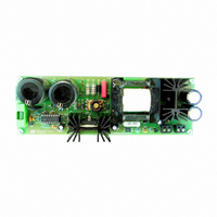
EVAL BOARD 3PH PWR SUPPLY W/ESBT
Manufacturer
STMicroelectronics
Type
DC/DC Switching Converters, Regulators & Controllersr
Datasheets
1.STC08DE150HP.pdf
(9 pages)
2.L5991AD13TR.pdf
(23 pages)
3.STEVAL-ISA007V1.pdf
(5 pages)
Specifications of STEVAL-ISA007V1
Mfg Application Notes
L5991 AppNote
Design Resources
STEVAL-ISA007V1 Gerber Files STEVAL-ISA007V1 Schematic STEVAL-ISA007V1 Bill of Materials
Main Purpose
AC/DC, Primary Side
Outputs And Type
2, Isolated
Power - Output
150W
Voltage - Output
24V, 5V
Current - Output
6.25A, 75mA
Voltage - Input
250 ~ 850V
Regulator Topology
Flyback
Frequency - Switching
90kHz
Board Type
Fully Populated
Utilized Ic / Part
L5991, STC08DE150
Input Voltage
400 V
Output Voltage
5 V, 24 V
Product
Power Management Modules
Lead Free Status / RoHS Status
Contains lead / RoHS non-compliant
For Use With/related Products
L5991, STC08DE150HV
Other names
497-5083


L5991 - L5991A
in fig.28) holds the pin low in order to ensure that
the external MOS cannot be turned on acciden-
tally. The peculiarity of this circuit is its ability to
mantain the same sink capability (typically, 20mA
@ 1V) from V
When the threshold is exceeded and the L5991
starts operating, V
28) and the circuit is disabled.
It is then possible to omit the "bleeder" resistor
(connected between the gate and the source of
the MOS) ordinarily used to prevent undesired
switching-on of the external MOS because of
some leakage current.
Figure 28. Pull-Down of the output in UVLO.
Pin 11. PGND (Power Ground). The current loop
during the discharge of the gate of the external
MOS is closed through this pin. This loop should
be as short as possible to reduce EMI and run
separately from signal currents return.
Pin 12. SGND (Signal Ground). This ground refer-
ences the control circuitry of the IC, so all the
ground connections of the external parts related
to control functions must lead to this pin. In laying
out the PCB, care must be taken in preventing
switched high currents from flowing through the
SGND path.
Figure 29. Internal LEB.
12/23
V
REFOK
CC
ISEN
= 0V up to the start-up threshold.
REFOK
13
is pulled high (refer to fig.
I
1.2V
0
D97IN538
+
-
3V
10
12
OVERCURRENT
COMPARATOR
OUT
SGND
FROM E/A
CLK
2V
+
+
-
-
Pin 13. ISEN (Current Sense). This pin is to be
connected to the "hot" lead of the current sense
resistor R
get a voltage ramp which is an image of the cur-
rent of the switch (I
to:
the conduction of the switch is terminated.
To increase the noise immunity, a "Leading Edge
Blanking" of about 100ns is internally realized as
shown in fig. 29. Because of that, the smoothing
RC filter between this pin and R
moved or, at least, considerably reduced.
Pin 14. DIS (Device Disable). When the voltage
on pin 14 rises above 2.5V the IC is shut down
and it is necessary to pull VCC (IC supply voltage,
pin 8) below the UVLO threshold to allow the de-
vice to restart.
The pin can be driven by an external logic signal
in case of power management, as shown in fig.
30. It is also possible to realize an overvoltage
protection, as shown in the section " Application
Ideas".If used, bypass this pin to ground with a fil-
ter capacitor to avoid spurious activation due to
noise spikes. If not, it must be connected to
SGND.
Pin 15. DC-LIM (Maximum Duty Cycle Limit). The
upper extreme, Dx, of the duty cycle range de-
pends on the voltage applied to this pin. Approxi-
mately,
if DC-LIM is grounded or left floating. Instead,
COMPARATOR
V
PWM
13pk
sense
I
Qpk
D
(being the other one grounded), to
x
D97IN503
R
Q
R
sense
). When this voltage is equal
T
R
T
230
TO FAULT
TO PWM
LOGIC
LOGIC
V
COMP
10
sense
3
1.4
could be re-
9
Related parts for STEVAL-ISA007V1
Image
Part Number
Description
Manufacturer
Datasheet
Request
R

Part Number:
Description:
BOARD RGB CTR ST7,STP08C596MTR
Manufacturer:
STMicroelectronics
Datasheet:

Part Number:
Description:
Power Management IC Development Tools Full Speed USB to RS232 Bridge Demo
Manufacturer:
STMicroelectronics
Datasheet:
Part Number:
Description:
Power Management IC Development Tools 2.5W solar eval BRD USB SPV1040 LD39050
Manufacturer:
STMicroelectronics
Datasheet:

Part Number:
Description:
BOARD EVAL FOR MEMS SENSORS
Manufacturer:
STMicroelectronics
Datasheet:

Part Number:
Description:
KIT DEV STARTER ST10F276Z5
Manufacturer:
STMicroelectronics
Datasheet:

Part Number:
Description:
BOARD EVAL HDMI $ VIDEO SWITCH
Manufacturer:
STMicroelectronics
Datasheet:

Part Number:
Description:
BOARD DEMO ACCELEROMETER DIL24
Manufacturer:
STMicroelectronics
Datasheet:

Part Number:
Description:
BOARD STLM75/STDS75/ST72F651
Manufacturer:
STMicroelectronics
Datasheet:

Part Number:
Description:
EVAL BOARD 3AXIS MEMS ACCELLRMTR
Manufacturer:
STMicroelectronics
Datasheet:

Part Number:
Description:
BOARD EVAL 8BIT MICRO + TDE1708
Manufacturer:
STMicroelectronics
Datasheet:
Part Number:
Description:
STMicroelectronics [RIPPLE-CARRY BINARY COUNTER/DIVIDERS]
Manufacturer:
STMicroelectronics
Datasheet:
Part Number:
Description:
STMicroelectronics [LIQUID-CRYSTAL DISPLAY DRIVERS]
Manufacturer:
STMicroelectronics
Datasheet:
Part Number:
Description:
BOARD EVAL FOR MEMS SENSORS
Manufacturer:
STMicroelectronics
Datasheet: