NCP3101BUCK1GEVB ON Semiconductor, NCP3101BUCK1GEVB Datasheet - Page 4
NCP3101BUCK1GEVB
Manufacturer Part Number
NCP3101BUCK1GEVB
Description
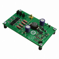
EVAL BOARD FOR NCP3101BUCK1G
Manufacturer
ON Semiconductor
Specifications of NCP3101BUCK1GEVB
Design Resources
NCP3101BUCK1 EVB BOM NCP3101BUCKL1GEVB Gerber Files NCP3101BUCK1 EVB Schematic
Main Purpose
DC/DC, Step Down
Outputs And Type
1, Non-Isolated
Voltage - Output
3.3V
Current - Output
6A
Voltage - Input
13.2V
Regulator Topology
Buck
Frequency - Switching
275kHz
Board Type
Fully Populated
Utilized Ic / Part
NCP3101
Lead Free Status / RoHS Status
Lead free / RoHS Compliant
Power - Output
-
Lead Free Status / Rohs Status
Lead free / RoHS Compliant
For Use With/related Products
NCP3101BUCK1G
Other names
NCP3101BUCK1GEVBOS


Stresses exceeding Maximum Ratings may damage the device. Maximum Ratings are stress ratings only. Functional operation above the
Recommended Operating Conditions is not implied. Extended exposure to stresses above the Recommended Operating Conditions may affect
device reliability.
NOTE:
1. 60−180 seconds minimum above 237°C
2. Based on 110 * 100 mm double layer PCB with 35 mm thick copper plating.
Table 2. ABSOLUTE MAXIMUM RATINGS
Bootstrap Pin Voltage vs V
High Side Switch Max DC Current
V
V
CPHASE Pin Voltage
CPHASE Pin Voltage (spikes < 50 ns)
Current Limit Set and Bottom Gate
Current Limit Set and Bottom Gate (spikes < 200 ns)
Top Gate vs Ground
Top Gate vs Phase
Top Gate vs Phase (spikes < 200 ns)
FB Pin Voltage
COMP/DISABLE
Thermal Resistance, Junction−to−Ambient (Note 2)
Thermal Resistance, Junction−to−Case (Note 2) at
85°C
Continuous Power Distribution (T
Storage Temperature Range
Junction Operating Temperature
Lead Temperature Soldering (10 sec):
Reflow (SMD styles only) Pb−Free (Note 1)
PWRPHS
PWRPHS
These devices have limited built−in ESD protection. The devices should be shorted together or the device placed in conductive
foam during storage or handling to prevent electrostatic damage to the device.
Pin Voltage
Pin Voltage (spikes < 50 ns)
Pin Name
Rating
PWRPHS
A
= +85°C)
http://onsemi.com
V
BST
VCOMP/DIS
V
V
V
PWRPHSSP
Symbol
Symbol
PWRPHS
V
V
V
CPHSTR
−V
I PHS
R
R
V
V
V
V
CPHS
BGSP
TGSP
T
P
RF
T
4
qJA
qJC
BG
TG
TG
stg
FB
PWRPHS
D
J
−0.3
−0.7
−0.7
−0.3
−2.0
−0.3
−0.3
−2.0
−0.3
−0.3
Min
−5
−5
0
V
−55 to 150
−40 to 150
CC
260 peak
V
V
Symbol
V
V
V
CC
CC
CC
< V
CC
1.8
CC
35
5
< V
< V
< V
COMP/DIS
< V
< V
Max
7.5
15
30
40
30
40
30
BGSP
TGSP
BG
FB
TG
< 6.0
< 15
< 15
< 15
< 15
< 6.0
°C/W
°C/W
Unit
Unit
°C
°C
°C
W
V
A
V
V
V
V
V
V
V
V
V
V
V
Related parts for NCP3101BUCK1GEVB
Image
Part Number
Description
Manufacturer
Datasheet
Request
R

Part Number:
Description:
Wide Input Voltage Synchronous Buck Converter
Manufacturer:
ON Semiconductor
Datasheet:
Part Number:
Description:
ON Semiconductor [VOLTAGE REGULATOR]
Manufacturer:
ON Semiconductor
Datasheet:
Part Number:
Description:
357-036-542-201 CARDEDGE 36POS DL .156 BLK LOPRO
Manufacturer:
ON Semiconductor
Datasheet:
Part Number:
Description:
357-036-542-201 CARDEDGE 36POS DL .156 BLK LOPRO
Manufacturer:
ON Semiconductor
Datasheet:
Part Number:
Description:
357-036-542-201 CARDEDGE 36POS DL .156 BLK LOPRO
Manufacturer:
ON Semiconductor
Datasheet:
Part Number:
Description:
357-036-542-201 CARDEDGE 36POS DL .156 BLK LOPRO
Manufacturer:
ON Semiconductor
Datasheet:
Part Number:
Description:
357-036-542-201 CARDEDGE 36POS DL .156 BLK LOPRO
Manufacturer:
ON Semiconductor
Datasheet:
Part Number:
Description:
357-036-542-201 CARDEDGE 36POS DL .156 BLK LOPRO
Manufacturer:
ON Semiconductor
Datasheet:
Part Number:
Description:
357-036-542-201 CARDEDGE 36POS DL .156 BLK LOPRO
Manufacturer:
ON Semiconductor
Datasheet:
Part Number:
Description:
357-036-542-201 CARDEDGE 36POS DL .156 BLK LOPRO
Manufacturer:
ON Semiconductor
Datasheet:
Part Number:
Description:
357-036-542-201 CARDEDGE 36POS DL .156 BLK LOPRO
Manufacturer:
ON Semiconductor
Datasheet:
Part Number:
Description:
357-036-542-201 CARDEDGE 36POS DL .156 BLK LOPRO
Manufacturer:
ON Semiconductor
Datasheet:
Part Number:
Description:
Manufacturer:
ON Semiconductor
Datasheet:
Part Number:
Description:
Manufacturer:
ON Semiconductor
Datasheet: