NCP3101BUCK1GEVB ON Semiconductor, NCP3101BUCK1GEVB Datasheet - Page 9
NCP3101BUCK1GEVB
Manufacturer Part Number
NCP3101BUCK1GEVB
Description
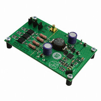
EVAL BOARD FOR NCP3101BUCK1G
Manufacturer
ON Semiconductor
Specifications of NCP3101BUCK1GEVB
Design Resources
NCP3101BUCK1 EVB BOM NCP3101BUCKL1GEVB Gerber Files NCP3101BUCK1 EVB Schematic
Main Purpose
DC/DC, Step Down
Outputs And Type
1, Non-Isolated
Voltage - Output
3.3V
Current - Output
6A
Voltage - Input
13.2V
Regulator Topology
Buck
Frequency - Switching
275kHz
Board Type
Fully Populated
Utilized Ic / Part
NCP3101
Lead Free Status / RoHS Status
Lead free / RoHS Compliant
Power - Output
-
Lead Free Status / Rohs Status
Lead free / RoHS Compliant
For Use With/related Products
NCP3101BUCK1G
Other names
NCP3101BUCK1GEVBOS


General
voltage 6 A synchronous PWM buck converter designed to
operate from a 4.5 V to 13.2 V supply. The output voltage of
the converter can be precisely regulated down to 800 mV
+1.0% when the VFB pin is tied to the output voltage. The
switching frequency is internally set to 275 kHz. A high gain
Operational Transconductance Error Amplifier (OTEA) is
used for feedback and stabilizing the loop.
Input Voltage
using the V
The PWRVCC pin provides voltage to the switching
MOSFETS. The V
circuitry and driver stage.
input voltage of the PWRVCC pin can accept 2.7 V to 18 V.
If the V
voltage range is 4.5 V to 13.2 V.
Duty Cycle and Maximum Pulse Width Limits
at an operating point defined by the ratio of the input to the
output voltage. The NCP3101C can achieve an 82% duty
ratio. The part has a built in off−time which ensures that the
bootstrap supply is charged every cycle. The NCP3101C is
capable of a 100 ns pulse width (minimum) and allows a
12 V to 0.8 V conversion at 275 kHz. The duty cycle limit
and the corresponding output voltage are shown below in
graphical format in Figure 18. The green area represents the
safe operating area for the lowest maximum operational
duty cycle for 4.5 V and 13.2 V.
Input voltage range (VCC and BST)
to 13.2 V with reference to GND and PHS, respectively.
12. 5
11. 5
10. 5
NCP3101C is a high efficiency integrated wide input
The NCP3101C can be used in many applications by
If the V
In steady state DC operation, the duty cycle will stabilize
The input voltage range for both VCC and BST is 4.5 V
9. 5
8. 5
7. 5
6. 5
5. 5
4. 5
3. 5
CC
Figure 18. Maximum Input to Output Voltage
CC
and PWRVCC pins are tied together the input
4. 5
CC
and the PWRVCC pin are not tied together, the
D
max
and PWRVCC pins together or separately.
5. 5
= 0.82
CC
OUTPUT VOLTAGE (V)
pin provides voltage to the control
6. 5
D
max
7. 5
= 0.88
8. 5
DETAILED OPERATING DESCRIPTION
9. 5
10. 5 11. 5
http://onsemi.com
9
Although BST is rated at 13.2 V with reference to PHS, it can
also tolerate 26.5 V with respect to GND.
External Enable/Disable
threshold at 3.82 V and V
starts to rise. The PWRPHS node is tri−stated until the
COMP voltage exceeds 830 mV. Once the 830 mV
threshold is exceeded, the part starts to switch and is
considered enabled. When the COMP pin voltage is pulled
below the 400 mV threshold, it disables the PWM logic, the
top MOSFET is driven off, and the bottom MOSFET is
driven on as shown in Figure 19. In the disabled mode, the
OTA output source current is reduced to 10 mA.
pin, an open collector or open drain drive should be used as
shown in Figure 20.
Power Sequencing
two general purpose bipolar junction transistors or
MOSFETs. An example of the power sequencing circuit
using the external components is shown in Figure 21.
Gate Signal Enable
Once the input voltage has exceeded the boost and UVLO
When disabling the NCP3101C using the COMP / Disable
Power sequencing can be achieved with NCP3101C using
Figure 19. Enable/Disable Driver State Diagram
NCP3101C
COMP
Figure 20. Recommended Disable Circuits
Disable
COMP
0.83 V
VSW
FB1
BG
TG
Figure 21. Power Sequencing
1.0V
CC
COMP
Base Signal
threshold at 4 V, the COMP pin
VIN
Disable
Enable
NCP3101C
COMP
VSW
FB1
COMP
3.3V
Related parts for NCP3101BUCK1GEVB
Image
Part Number
Description
Manufacturer
Datasheet
Request
R

Part Number:
Description:
Wide Input Voltage Synchronous Buck Converter
Manufacturer:
ON Semiconductor
Datasheet:
Part Number:
Description:
ON Semiconductor [VOLTAGE REGULATOR]
Manufacturer:
ON Semiconductor
Datasheet:
Part Number:
Description:
357-036-542-201 CARDEDGE 36POS DL .156 BLK LOPRO
Manufacturer:
ON Semiconductor
Datasheet:
Part Number:
Description:
357-036-542-201 CARDEDGE 36POS DL .156 BLK LOPRO
Manufacturer:
ON Semiconductor
Datasheet:
Part Number:
Description:
357-036-542-201 CARDEDGE 36POS DL .156 BLK LOPRO
Manufacturer:
ON Semiconductor
Datasheet:
Part Number:
Description:
357-036-542-201 CARDEDGE 36POS DL .156 BLK LOPRO
Manufacturer:
ON Semiconductor
Datasheet:
Part Number:
Description:
357-036-542-201 CARDEDGE 36POS DL .156 BLK LOPRO
Manufacturer:
ON Semiconductor
Datasheet:
Part Number:
Description:
357-036-542-201 CARDEDGE 36POS DL .156 BLK LOPRO
Manufacturer:
ON Semiconductor
Datasheet:
Part Number:
Description:
357-036-542-201 CARDEDGE 36POS DL .156 BLK LOPRO
Manufacturer:
ON Semiconductor
Datasheet:
Part Number:
Description:
357-036-542-201 CARDEDGE 36POS DL .156 BLK LOPRO
Manufacturer:
ON Semiconductor
Datasheet:
Part Number:
Description:
357-036-542-201 CARDEDGE 36POS DL .156 BLK LOPRO
Manufacturer:
ON Semiconductor
Datasheet:
Part Number:
Description:
357-036-542-201 CARDEDGE 36POS DL .156 BLK LOPRO
Manufacturer:
ON Semiconductor
Datasheet:
Part Number:
Description:
Manufacturer:
ON Semiconductor
Datasheet:
Part Number:
Description:
Manufacturer:
ON Semiconductor
Datasheet: