NCP1606BOOSTGEVB ON Semiconductor, NCP1606BOOSTGEVB Datasheet - Page 12
NCP1606BOOSTGEVB
Manufacturer Part Number
NCP1606BOOSTGEVB
Description
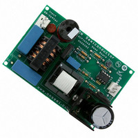
EVAL BOARD FOR NCP1606BOOSTG
Manufacturer
ON Semiconductor
Specifications of NCP1606BOOSTGEVB
Design Resources
NCP1606BOOST EVB BOM NCP1606BOOSTGEVB Gerber Files NCP1606BOOST EVB Schematic
Main Purpose
AC/DC, Primary and Secondary Side with PFC
Outputs And Type
1, Isolated
Power - Output
100W
Voltage - Output
400V
Current - Output
250mA
Voltage - Input
88 ~ 264VAC
Regulator Topology
Boost
Frequency - Switching
250kHz
Board Type
Fully Populated
Utilized Ic / Part
NCP1606
Lead Free Status / RoHS Status
Lead free / RoHS Compliant
For Use With/related Products
NCP1606BOOSTG
Other names
NCP1606BOOSTGEVBOS


the average demand only. Therefore, the output capacitor
must “absorb” the difference between the delivered power
and the power consumed by the load. This means that when
the power fed to the load is lower than the demand, the
output capacitor discharges to compensate for the lack of
a frequency of either 100 Hz (for 50 Hz mains such as in
Europe) or 120 Hz (for 60 Hz mains in the USA). This
ripple must not be taken into account by the regulation loop
because the error amplifier’s output voltage must be kept
constant over a given ac line cycle for a proper shaping of
the line current. Due to this constraint, the regulation
bandwidth is typically set below 20 Hz. For a simple type 1
compensation network, only a capacitor is placed between
FB and Control (see Figure 1). In this configuration, the
capacitor necessary to attenuate the bulk voltage ripple is
given by:
where G is the attenuation level in dB (commonly 60 dB)
ON TIME SEQUENCE
converter, its switching pattern must accommodate
constant on times and variable off times. The Controller
generates the on time via an external capacitor connected
to pin 3 (Ct). A current source charges this capacitor to a
level determined by the Control pin voltage. Specifically,
Ct is charged to V
(typically 2.1 V). Once this level is exceeded, the drive is
turned off (Figure 27).
As a consequence, the output voltage exhibits a ripple at
Since the NCP1606 is designed to control a CRM boost
C
COMP
CONTROL
+
4 @ p f
Figure 26. Output Voltage Ripple for a Constant Output Power
line
10
P
minus the V
V
IN
20
@ R
OUT
G
OUT1
P
OUT
Vac
Iac
EAL
http://onsemi.com
(eq. 3)
offset
12
power. Alternatively, when the supplied power is higher
than that absorbed by the load, the output capacitor charges
to store the excess energy. The situation is depicted in
Figure 26.
output load, this naturally satisfies equation 1. And if the
values of compensation components are sufficient to filter
Since V
Control
Ct
CONTROL
Figure 27. On Time Generation
V
DD
I
V
CHARGE
varies with the RMS line level and
Ct(off)
DRV
DRV
V
CONTROL
V
V
Ct
CONTROL
t
ON
V
+
EAL
− V
PWM
+
EAL
−
t
ON
Related parts for NCP1606BOOSTGEVB
Image
Part Number
Description
Manufacturer
Datasheet
Request
R

Part Number:
Description:
Cost Effective Power Factor Controller
Manufacturer:
ON Semiconductor
Datasheet:
Part Number:
Description:
ON Semiconductor [VOLTAGE REGULATOR]
Manufacturer:
ON Semiconductor
Datasheet:
Part Number:
Description:
357-036-542-201 CARDEDGE 36POS DL .156 BLK LOPRO
Manufacturer:
ON Semiconductor
Datasheet:
Part Number:
Description:
357-036-542-201 CARDEDGE 36POS DL .156 BLK LOPRO
Manufacturer:
ON Semiconductor
Datasheet:
Part Number:
Description:
357-036-542-201 CARDEDGE 36POS DL .156 BLK LOPRO
Manufacturer:
ON Semiconductor
Datasheet:
Part Number:
Description:
357-036-542-201 CARDEDGE 36POS DL .156 BLK LOPRO
Manufacturer:
ON Semiconductor
Datasheet:
Part Number:
Description:
357-036-542-201 CARDEDGE 36POS DL .156 BLK LOPRO
Manufacturer:
ON Semiconductor
Datasheet:
Part Number:
Description:
357-036-542-201 CARDEDGE 36POS DL .156 BLK LOPRO
Manufacturer:
ON Semiconductor
Datasheet:
Part Number:
Description:
357-036-542-201 CARDEDGE 36POS DL .156 BLK LOPRO
Manufacturer:
ON Semiconductor
Datasheet:
Part Number:
Description:
357-036-542-201 CARDEDGE 36POS DL .156 BLK LOPRO
Manufacturer:
ON Semiconductor
Datasheet:
Part Number:
Description:
357-036-542-201 CARDEDGE 36POS DL .156 BLK LOPRO
Manufacturer:
ON Semiconductor
Datasheet:
Part Number:
Description:
357-036-542-201 CARDEDGE 36POS DL .156 BLK LOPRO
Manufacturer:
ON Semiconductor
Datasheet:
Part Number:
Description:
Manufacturer:
ON Semiconductor
Datasheet:
Part Number:
Description:
Manufacturer:
ON Semiconductor
Datasheet: