NCP1606BOOSTGEVB ON Semiconductor, NCP1606BOOSTGEVB Datasheet - Page 16
NCP1606BOOSTGEVB
Manufacturer Part Number
NCP1606BOOSTGEVB
Description
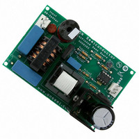
EVAL BOARD FOR NCP1606BOOSTG
Manufacturer
ON Semiconductor
Specifications of NCP1606BOOSTGEVB
Design Resources
NCP1606BOOST EVB BOM NCP1606BOOSTGEVB Gerber Files NCP1606BOOST EVB Schematic
Main Purpose
AC/DC, Primary and Secondary Side with PFC
Outputs And Type
1, Isolated
Power - Output
100W
Voltage - Output
400V
Current - Output
250mA
Voltage - Input
88 ~ 264VAC
Regulator Topology
Boost
Frequency - Switching
250kHz
Board Type
Fully Populated
Utilized Ic / Part
NCP1606
Lead Free Status / RoHS Status
Lead free / RoHS Compliant
For Use With/related Products
NCP1606BOOSTG
Other names
NCP1606BOOSTGEVBOS


R
equilibrium
compensation capacitor (“C
•
where (V
•
•
Conversely when V
output of the error amplifier sinks or sources the current
necessary to maintain 2.5 V on pin 1. In particular, in the
case of an overvoltage condition:
•
•
I
OUT2
When the output voltage is in steady state, R
R
Under stable conditions, these equations are true.
where DV
The R
The R
And since no current flows through C
The error amplifier maintains 2.5 V on pin 1, and the
R
The R
I
OUT1
R
R
OUT2
R
OUT1
OUT1
OUT2
V
+I
regulate the FB voltage to 2.5 V. Also, during this
OUT
OUT1
OUT2
OUT1
OUT
+
current remains:
R
OUT2
V
OUT
)
OUT
state, no current flows through the
current is:
nom
current is:
current is:
I
R
R
å
OUT1
Control
OUT1
is the output voltage excess.
−2.5 V
is the nominal output voltage.
(V
C
OUT
COMP
FB
I
I
+
OUT
R
R
OUT2
OUT2
(V
+
)
R
is not at its nominal level, the
nom
OUT
OUT1
(V
+
+
COMP
OUT
* 2.5 V
)
R
R
R
2.5 V
2.5 V
nom
OUT1
OUT2
OUT2
” of Figure 1). Therefore:
)
nom
* 2.5 V
R
) DV
+
I
V
CONTROL
+
OUT1
CONTROL
Figure 34. OVP and UVP Circuit Blocks
COMP
+
R
2.5 V
OUT2
OUT
300 mV
E/A
,
2.5 V
+
+
−
−
−2.5 V
OUT1
(eq. 10)
http://onsemi.com
UVP
(eq. 6)
(eq. 7)
(eq. 8)
(eq. 9)
and
Enable
(Enable EA)
16
•
simple expression of the current sunk by the error
amplifier:
proportional to the output voltage excess. The circuit
senses this current and disables the drive (pin 7) when
I
10.4 mA in NCP1606B). This gives the OVP threshold as:
set. Therefore, one can compute the R
resistances using the following procedure:
CONTROL
The combination of Equations 2 and 11 leads to a very
Hence, the current absorbed by pin 2 (I
By simply adjusting R
I
Therefore, the error amplifier sinks:
Measure
I
CONTROL
R
Clamp
1. Select R
2. Select R
Clamp
OUT1
V
V
V
EAL
EAH
DD
For instance if implementing the NCP1606B, and
420 V is the maximum output level and 400 V is the
nominal output level, then
(V
−I
I
OUT
CONTROL
R
exceeds I
Static OVP
R
Static OVP is triggered
when clamp is activated.
OUT2
Dynamic OVP
I
CONTROL
OUT1
)
R
OVP
R
OUT1
OUT1
OUT2
+
OUT2
+
+ (V
(V
+ I
OVP
+ 420 * 400
> I
to set the desired overvoltage level:
(V
to adjust the regulation level:
OUT
+
R
ovp
OUT
OUT
OUT1
OUT1
V
)
(typically 40 mA in NCP1606A,
10.4 mA
nom
OUT(nom)
2.5 V @ R
)
)
OVP
nom
* I
R
, the OVP limit can be easily
) DV
I
OUT1
OVP
R
* (V
) (R
OUT2
* 2.5 V
+ 1.9 MW
OUT
OUT1
OUT
OUT1
+
−2.5 V
OUT1
DV
)
R
nom
OUT1
@ I
OUT
Fault
CONTROL
OVP
−
and R
R
2.5 V
)
OUT2
(eq. 12)
(eq. 11)
OUT2
) is
Related parts for NCP1606BOOSTGEVB
Image
Part Number
Description
Manufacturer
Datasheet
Request
R

Part Number:
Description:
Cost Effective Power Factor Controller
Manufacturer:
ON Semiconductor
Datasheet:
Part Number:
Description:
ON Semiconductor [VOLTAGE REGULATOR]
Manufacturer:
ON Semiconductor
Datasheet:
Part Number:
Description:
357-036-542-201 CARDEDGE 36POS DL .156 BLK LOPRO
Manufacturer:
ON Semiconductor
Datasheet:
Part Number:
Description:
357-036-542-201 CARDEDGE 36POS DL .156 BLK LOPRO
Manufacturer:
ON Semiconductor
Datasheet:
Part Number:
Description:
357-036-542-201 CARDEDGE 36POS DL .156 BLK LOPRO
Manufacturer:
ON Semiconductor
Datasheet:
Part Number:
Description:
357-036-542-201 CARDEDGE 36POS DL .156 BLK LOPRO
Manufacturer:
ON Semiconductor
Datasheet:
Part Number:
Description:
357-036-542-201 CARDEDGE 36POS DL .156 BLK LOPRO
Manufacturer:
ON Semiconductor
Datasheet:
Part Number:
Description:
357-036-542-201 CARDEDGE 36POS DL .156 BLK LOPRO
Manufacturer:
ON Semiconductor
Datasheet:
Part Number:
Description:
357-036-542-201 CARDEDGE 36POS DL .156 BLK LOPRO
Manufacturer:
ON Semiconductor
Datasheet:
Part Number:
Description:
357-036-542-201 CARDEDGE 36POS DL .156 BLK LOPRO
Manufacturer:
ON Semiconductor
Datasheet:
Part Number:
Description:
357-036-542-201 CARDEDGE 36POS DL .156 BLK LOPRO
Manufacturer:
ON Semiconductor
Datasheet:
Part Number:
Description:
357-036-542-201 CARDEDGE 36POS DL .156 BLK LOPRO
Manufacturer:
ON Semiconductor
Datasheet:
Part Number:
Description:
Manufacturer:
ON Semiconductor
Datasheet:
Part Number:
Description:
Manufacturer:
ON Semiconductor
Datasheet: