NCP1351ADAPGEVB ON Semiconductor, NCP1351ADAPGEVB Datasheet - Page 7
NCP1351ADAPGEVB
Manufacturer Part Number
NCP1351ADAPGEVB
Description
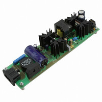
EVAL BOARD FOR NCP1351ADAPG
Manufacturer
ON Semiconductor
Datasheets
1.NCP1351APG.pdf
(27 pages)
2.NCP1351ADAPGEVB.pdf
(10 pages)
3.NCP1351ADAPGEVB.pdf
(1 pages)
Specifications of NCP1351ADAPGEVB
Design Resources
NCP1351 Adapter EVB BOM NCP1351ADAPGEVB Gerber Files NCP1351 Adapter EVB Schematic
Main Purpose
AC/DC, Primary Side
Outputs And Type
1, Isolated
Power - Output
57W
Voltage - Output
19V
Current - Output
3A
Voltage - Input
90 ~ 265VAC
Regulator Topology
Flyback
Frequency - Switching
65kHz
Board Type
Fully Populated
Utilized Ic / Part
NCP1351
Lead Free Status / RoHS Status
Lead free / RoHS Compliant
Other names
NCP1351ADAPGEVBOS


Stresses exceeding Maximum Ratings may damage the device. Maximum Ratings are stress ratings only. Functional operation above the
Recommended Operating Conditions is not implied. Extended exposure to stresses above the Recommended Operating Conditions may affect
device reliability.
NOTE:
MAXIMUM RATINGS
V
Symbol
I
SUPPLY
I
T
R
SUPPLY
V
V
FBmax
I
I
R
JMAX
DRV
MAX
MAX
Gmin
DRV
qJA
This device contains latchup protection and exceeds 100 mA per JEDEC Standard JESD78.
Maximum Supply on V
Maximum Current in V
Maximum Voltage on DRV Pin 5
Maximum Current in DRV Pin 5
Supply Voltage on all pins, except Pin 6 (V
Maximum Current in all Pins Except Pin 6 (V
Maximum Injected Current in Pin 1 (FB)
Minimum Resistive Load on DRV Pin
Thermal Resistance Junction-to-Air
Maximum Junction Temperature
Storage Temperature Range
ESD Capability, Human Body Model V per Mil-STD-883, Method 3015
ESD Capability, Machine Model
CC
CC
Pin 6
Pin 6
Rating
CC
CC
), Pin 5 (DRV)
http://onsemi.com
) and Pin 5 (DRV)
NCP1351
7
SOIC-8
PDIP-8
-60 to +150
-0.3 to 28
-0.3 to 20
-0.3 to 10
$400
Value
$10
142
176
150
200
0.5
20
33
2
°C/W
Unit
mA
mA
mA
mA
kW
°C
°C
kV
V
V
V
V
Related parts for NCP1351ADAPGEVB
Image
Part Number
Description
Manufacturer
Datasheet
Request
R

Part Number:
Description:
ON Semiconductor [VOLTAGE REGULATOR]
Manufacturer:
ON Semiconductor
Datasheet:
Part Number:
Description:
357-036-542-201 CARDEDGE 36POS DL .156 BLK LOPRO
Manufacturer:
ON Semiconductor
Datasheet:
Part Number:
Description:
357-036-542-201 CARDEDGE 36POS DL .156 BLK LOPRO
Manufacturer:
ON Semiconductor
Datasheet:
Part Number:
Description:
357-036-542-201 CARDEDGE 36POS DL .156 BLK LOPRO
Manufacturer:
ON Semiconductor
Datasheet:
Part Number:
Description:
357-036-542-201 CARDEDGE 36POS DL .156 BLK LOPRO
Manufacturer:
ON Semiconductor
Datasheet:
Part Number:
Description:
357-036-542-201 CARDEDGE 36POS DL .156 BLK LOPRO
Manufacturer:
ON Semiconductor
Datasheet:
Part Number:
Description:
357-036-542-201 CARDEDGE 36POS DL .156 BLK LOPRO
Manufacturer:
ON Semiconductor
Datasheet:
Part Number:
Description:
357-036-542-201 CARDEDGE 36POS DL .156 BLK LOPRO
Manufacturer:
ON Semiconductor
Datasheet:
Part Number:
Description:
357-036-542-201 CARDEDGE 36POS DL .156 BLK LOPRO
Manufacturer:
ON Semiconductor
Datasheet:
Part Number:
Description:
357-036-542-201 CARDEDGE 36POS DL .156 BLK LOPRO
Manufacturer:
ON Semiconductor
Datasheet:
Part Number:
Description:
357-036-542-201 CARDEDGE 36POS DL .156 BLK LOPRO
Manufacturer:
ON Semiconductor
Datasheet:
Part Number:
Description:
Manufacturer:
ON Semiconductor
Datasheet:
Part Number:
Description:
Manufacturer:
ON Semiconductor
Datasheet: