NCP1351ADAPGEVB ON Semiconductor, NCP1351ADAPGEVB Datasheet - Page 8
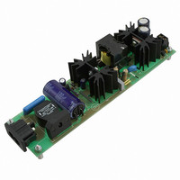
NCP1351ADAPGEVB
Manufacturer Part Number
NCP1351ADAPGEVB
Description
EVAL BOARD FOR NCP1351ADAPG
Manufacturer
ON Semiconductor
Datasheets
1.NCP1351APG.pdf
(27 pages)
2.NCP1351ADAPGEVB.pdf
(10 pages)
3.NCP1351ADAPGEVB.pdf
(1 pages)
Specifications of NCP1351ADAPGEVB
Design Resources
NCP1351 Adapter EVB BOM NCP1351ADAPGEVB Gerber Files NCP1351 Adapter EVB Schematic
Main Purpose
AC/DC, Primary Side
Outputs And Type
1, Isolated
Power - Output
57W
Voltage - Output
19V
Current - Output
3A
Voltage - Input
90 ~ 265VAC
Regulator Topology
Flyback
Frequency - Switching
65kHz
Board Type
Fully Populated
Utilized Ic / Part
NCP1351
Lead Free Status / RoHS Status
Lead free / RoHS Compliant
Other names
NCP1351ADAPGEVBOS


1. Guaranteed by design.
Electrical Characteristics
unless otherwise noted)
SUPPLY SECTION AND V
CURRENT SENSE
TIMING CAPACITOR
FEEDBACK SECTION
DRIVE OUTPUT
Protection
VCC
VCC
ICC
V
V
VCT
Symbol
V
V
VCT
VCC
I
V
V
T
V
K
T
I
I
I
FBcomp
I
I
I
OFFSET
I
DRVhigh
CSmax
CSmax
ICC1
ICC2
ICC3
ICC4
CSmin
CSmin
t
FAULT
DRVlow
TIMER
ZENER
DISCH
FBred
R
TIMER
TIMER
LATCH
V
FAULT
FAULT
R
delay
V
I
LATCH
T
T
CT
TH
OH
FB
OL
STOP
HYST
MAX
r
MIN
f
ON
V
V
Hysteresis VCC
Clamped V
Startup Current
Internal IC Consumption with I
Internal IC Consumption with I
Internal IC Consumption in Auto-Recovery Latch-off Phase
Current Flowing into V
Minimum Source Current (I
Minimum Source Current (I
Maximum Source Current (I
Maximum Source Current (I
Current Sense Comparator Threshold Voltage
Propagation Time Delay (CS Falling Edge to Gate Output)
Minimum Voltage on C
Voltage on C
Source Current (Ct Pin Grounded)
Minimum Voltage on C
C
C
Factor Linking V
FB Pin Voltage for an Injected Current of 200 mA
FB Current Under Which a Fault is Detected
FB Current at Which CS Compression Starts
FB Current at Which CS Compression is Finished
Output Voltage Rise-time @ CL = 1 nF, 10 - 90% of Output Signal
Output Voltage Fall-time @ CL = 1 nF, 10 - 90% of Output Signal
Source Resistance
Sink Resistance
DRV Pin Level at V
DRV Pin Level at V
Timing Capacitor Charging Current
Fault Voltage on Pin 8
Fault Timer Duration, C
Latching Voltage
CC
CC
T
T
Capacitor Discharge Time (Activated at DRV Turn-on)
Capacitor Level at Which Fault Timer Starts
Increasing Level at Which Driving Pulses are Authorized
Decreasing Level at Which Driving Pulses are Stopped
CC
T
CC
When Latched Off
Capacitor at I
ON
OFFSET
MANAGEMENT
(For typical values T
CC
CC
- VCC
CC
T
T
Close to VCC
= 28 V with 33 kW Resistor to GND
TIMER
, Discharge Switch Activated
and V
Capacitor, I
pin that Keeps the Controller Latched
STOP
FB
FB
FB
FB
FB
= 100 nF
= 90 mA)
= 90 mA)
FB
FB
FAULT
= 50 mA)
= 50 mA)
= 150 mA
= 50 mA, F
= 50 mA, F
Rating
FB
STOP
(Note 1)
J
= 30 mA
= 25°C, for Min/Max Values T
with a 33 kW Resistor to GND
SW
SW
http://onsemi.com
= 65 kHz and C
= 65 kHz and C
NCP1351
T
T
T
J
J
J
T
T
= -25°C to +125°C
= -25°C to +125°C
= -25°C to +125°C
J
J
C and D Versions
A and B Versions
A and B Versions
8
= 0°C to +125°C
= 0°C to +125°C
C and D Version
C and D Version
T
J
L
L
= 25°C
= 0
= 1 nF
J
= -25°C to +125°C, Max T
Pin
6
6
6
6
6
6
6
6
6
3
3
3
3
3
3
2
2
2
2
2
2
-
1
1
1
1
5
5
5
5
5
5
8
8
-
7
1.67
Min
251
242
475
8.3
9.8
9.3
0.4
8.0
4.5
4.5
15
20
61
58
10
15
10
6
-
-
-
-
-
-
5
-
-
-
-
-
-
-
-
-
-
-
-
J
10.8
10.8
0.96
1.86
11.5
Typ
600
270
270
160
510
100
8.9
1.0
1.6
0.5
0.7
18
70
70
20
40
51
60
80
90
80
30
17
42
= 150°C, V
-
6
-
-
-
-
1
-
5
5
Max
2.05
11.8
11.9
289
289
300
565
9.5
1.8
2.5
0.6
5.5
5.5
22
10
75
75
35
20
20
13
-
-
-
-
-
-
-
-
-
-
-
-
-
-
-
-
-
CC
= 12 V
Unit
mA
mA
mV
mV
mV
ms
mA
mA
mA
mA
mA
mA
mA
mA
mA
mA
mA
mA
ns
ms
ns
ns
W
W
V
V
V
V
V
V
V
V
V
V
V
Related parts for NCP1351ADAPGEVB
Image
Part Number
Description
Manufacturer
Datasheet
Request
R

Part Number:
Description:
ON Semiconductor [VOLTAGE REGULATOR]
Manufacturer:
ON Semiconductor
Datasheet:
Part Number:
Description:
357-036-542-201 CARDEDGE 36POS DL .156 BLK LOPRO
Manufacturer:
ON Semiconductor
Datasheet:
Part Number:
Description:
357-036-542-201 CARDEDGE 36POS DL .156 BLK LOPRO
Manufacturer:
ON Semiconductor
Datasheet:
Part Number:
Description:
357-036-542-201 CARDEDGE 36POS DL .156 BLK LOPRO
Manufacturer:
ON Semiconductor
Datasheet:
Part Number:
Description:
357-036-542-201 CARDEDGE 36POS DL .156 BLK LOPRO
Manufacturer:
ON Semiconductor
Datasheet:
Part Number:
Description:
357-036-542-201 CARDEDGE 36POS DL .156 BLK LOPRO
Manufacturer:
ON Semiconductor
Datasheet:
Part Number:
Description:
357-036-542-201 CARDEDGE 36POS DL .156 BLK LOPRO
Manufacturer:
ON Semiconductor
Datasheet:
Part Number:
Description:
357-036-542-201 CARDEDGE 36POS DL .156 BLK LOPRO
Manufacturer:
ON Semiconductor
Datasheet:
Part Number:
Description:
357-036-542-201 CARDEDGE 36POS DL .156 BLK LOPRO
Manufacturer:
ON Semiconductor
Datasheet:
Part Number:
Description:
357-036-542-201 CARDEDGE 36POS DL .156 BLK LOPRO
Manufacturer:
ON Semiconductor
Datasheet:
Part Number:
Description:
357-036-542-201 CARDEDGE 36POS DL .156 BLK LOPRO
Manufacturer:
ON Semiconductor
Datasheet:
Part Number:
Description:
Manufacturer:
ON Semiconductor
Datasheet:
Part Number:
Description:
Manufacturer:
ON Semiconductor
Datasheet: