STEVAL-ISA063V1 STMicroelectronics, STEVAL-ISA063V1 Datasheet
STEVAL-ISA063V1
Specifications of STEVAL-ISA063V1


Related parts for STEVAL-ISA063V1


STEVAL-ISA063V1 Summary of contents
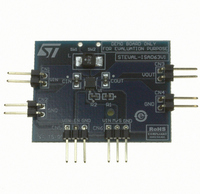
Page 1
Features ■ Buck-boost DC-DC converter ■ Operating input voltage range from 2 5.5 V ■ feedback voltage tolerance ■ Synchronous rectification ■ Shutdown function ■ 1.5 MHz switching frequency ■ Power save mode at light load ...
Page 2
Contents Contents 1 Block diagram . . . . . . . . . . . . . . . . . . . . . . . . . . . . . . . . . . . ...
Page 3
STBB1XX 1 Block diagram Figure 1. STBB1 block diagram Oscillator Oscillator VINA VINA DEVICE DEVICE MODE/SYNC MODE/SYNC CONTROL CONTROL EN EN SW1 SW1 Control Control Current Current sensor sensor Modulator Modulator Temp. Temp. Control Control GND ...
Page 4
Absolute maximum ratings 2 Absolute maximum ratings Table 2. Absolute maximum ratings Symbol VINA, VIN Input voltage VOUT Output voltage SW1, SW2 DC voltage FB DC voltage MOD/SYNC voltage T Maximum junction temperature J T Storage temperature range ...
Page 5
STBB1XX 3 Pin configuration Figure 2. Pin connections (top through view) Table 4. Pin description Pin n° Symbol 1 VOUT 2 SW2 3 PGND 4 SW1 5 VIN 6 EN MODE 7 (SYNC) 8 VINA 9 GND 10 FB Exposed ...
Page 6
Typical application 4 Typical application Figure 3. Application circuit - adjustable output version VIN VIN CIN CIN Figure 4. Application circuit - fixed output version VIN VIN CIN CIN Table 5. List of external components Component Manufacturer CIN Murata COUT ...
Page 7
STBB1XX 5 Electrical characteristics INA EN otherwise specified; typical values are referred to T Table 6. Electrical characteristics Symbol Parameter V Input voltage range IN V Under voltage lockout threshold UVLO V Feedback voltage ...
Page 8
Electrical characteristics Table 6. Electrical characteristics (continued) Symbol Parameter Efficiency 3 ν Thermal shutdown SHDN T Thermal shutdown hysteresis HYS 8/21 Test conditions mA OUT MODE ...
Page 9
STBB1XX 6 Detailed description 6.1 General description The STBB1 is a high efficiency dual mode buck-boost switch mode converter. Thanks to the 4 internal switches, 2 P-channel and 2 N-channel, and its unique control mechanisms it is able to deliver ...
Page 10
Detailed description 6.3 External synchronization The STBB1 implements external synchronization pin. If and external clock signal is applied to the MODE (SYN) pin with a frequency between 1.35 MHz and 2.0 MHz and with proper low/high levels, the device automatically ...
Page 11
STBB1XX 7 Typical performance characteristics L = 2.2 µ 3.3 V, all measurements done with circuit shown in O components listed in Figure 5. Efficiency vs. I OUT 100 100 ...
Page 12
Typical performance characteristics Figure 11. Boost region operation SW1 SW1 3 V/div 3 V/div SW2 SW2 3 V/div 3 V/div 0.2 A/div 0.2 A/div mV/div 20 mV/div AC Coupled AC Coupled ...
Page 13
STBB1XX 8 Application information 8.1 Programming the output voltage The STBB1 is available in two versions: fixed output voltage (STBB1PURXX) and adjustable output voltage (STBB1PUR). In the first case the device integrates the resistor divider needed to set the correct ...
Page 14
Application information The minimum inductor value for the application is the higher between Equation addition to the inductance value the maximum current the inductor can handle must be calculated in order to avoid saturation. Equation 4 = ...
Page 15
STBB1XX 9 Recommended PCB layout Figure 17. Component placement Figure 18. Top layer routing Figure 19. Bottom layer routing Doc ID 15474 Rev 5 Recommended PCB layout 15/21 ...
Page 16
Package mechanical data 10 Package mechanical data In order to meet environmental requirements, ST offers these devices in different grades of ECOPACK® packages, depending on their level of environmental compliance. ECOPACK® specifications, grade definitions and product status are available at: ...
Page 17
STBB1XX Dim. Min 0.18 D 2.85 D2 2.20 E 2. 0.30 ddd DFN10 (3x3 mm) mechanical data mm. Typ. Max. 0.90 1.00 0.02 0.05 0.65 0.80 0.20 0.25 0.30 ...
Page 18
Package mechanical data Tape & reel QFNxx/DFNxx (3x3) mechanical data Dim. Min 12 18/21 mm. Typ. Max. Min. 180 13.2 0.504 0.795 2.362 14.4 3.3 3.3 1.1 4 ...
Page 19
STBB1XX 11 Different output voltage versions of the STBB1 available on request Table 7. Options available on request Order codes STBB1PUR18 STBB1PUR25 STBB1PUR28 STBB1PUR33 Different output voltage versions of the STBB1 available on request Marking BB1 18 BB1 25 BB1 ...
Page 20
Revision history 12 Revision history Table 8. Document revision history Date Revision 19-Mar-2009 1 25-Mar-2009 2 01-Apr-2009 3 15-Jul-2009 4 07-Sep-2010 5 20/21 First release. Modified: Figure 5 and Figure 7 on page Modified: Figure 3 and Figure 4 on ...
Page 21
... STBB1XX Information in this document is provided solely in connection with ST products. STMicroelectronics NV and its subsidiaries (“ST”) reserve the right to make changes, corrections, modifications or improvements, to this document, and the products and services described herein at any time, without notice. All ST products are sold pursuant to ST’s terms and conditions of sale. ...