EVL6566A-75WADP STMicroelectronics, EVL6566A-75WADP Datasheet - Page 18
EVL6566A-75WADP
Manufacturer Part Number
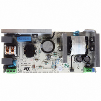
EVL6566A-75WADP
Description
BOARD EVAL FOR L6566A
Manufacturer
STMicroelectronics
Type
Power Factor Correctionr
Datasheets
1.L6566ATR.pdf
(51 pages)
2.TSM1014IDT.pdf
(10 pages)
3.L6563ATR.pdf
(39 pages)
4.EVL6566A-75WADP.pdf
(8 pages)
Specifications of EVL6566A-75WADP
Main Purpose
AC/DC, Primary and Secondary Side with PFC
Outputs And Type
1, Isolated
Power - Output
75W
Voltage - Output
19V
Current - Output
4A
Voltage - Input
90 ~ 264VAC
Frequency - Switching
65kHz
Board Type
Fully Populated
Utilized Ic / Part
L6563, L6566A, TSM1014
Input Voltage
90 V to 264 V
Output Voltage
19 V
Dimensions
78 mm x 174 mm
Product
Power Management Modules
Lead Free Status / RoHS Status
Lead free / RoHS Compliant
Regulator Topology
-
Lead Free Status / Rohs Status
Lead free / RoHS Compliant
For Use With/related Products
L6563, L6566A
Other names
497-6449
Available stocks
Company
Part Number
Manufacturer
Quantity
Price


Application information
6.2
6.3
18/39
Feedback Failure Protection (FFP)
The OVP function above described is able to handle "normal" overvoltage conditions, i.e.
those resulting from an abrupt load/line change or occurring at start-up. It cannot handle the
overvoltage generated, for instance, when the upper resistor of the output divider (R1) fails
open: the voltage loop can no longer read the information on the output voltage and will
force the PFC pre-regulator to work at maximum ON-time, causing the output voltage to rise
with no control.
A pin of the device (PFC_OK) has been dedicated to provide an additional monitoring of the
output voltage with a separate resistor divider (R3 high, R4 low, see
is selected so that the voltage at the pin reaches 2.5V if the output voltage exceeds a preset
value, usually larger than the maximum Vo that can be expected, also including worst-case
load/line transients.
Example: V
then: R4 = 3MΩ ·2.5/(475-2.5) = 15.87kΩ.
When this function is triggered, the gate drive activity is immediately stopped, the device is
shut down, its quiescent consumption is reduced below 250 µA and the condition is latched
as long as the supply voltage of the IC is above the UVLO threshold. At the same time the
pin PWM_LATCH is asserted high. PWM_LATCH is an open source output able to deliver
3.7V min. with 0.5 mA load, intended for tripping a latched shutdown function of the PWM
controller IC in the cascaded DC-DC converter, so that the entire unit is latched off. To
restart the system it is necessary to recycle the input power, so that the Vcc voltages of both
the L6563/A and the PWM controller go below their respective UVLO thresholds.
The PFC_OK pin doubles its function as a not-latched IC disable: a voltage below 0.2V will
shut down the IC, reducing its consumption below 1 mA. In this case both PWM_STOP and
PWM_LATCH keep their high impedance status. To restart the IC simply let the voltage at
the pin go above 0.26 V.
Note that this function offers a complete protection against not only feedback loop failures or
erroneous settings, but also against a failure of the protection itself. Either resistor of the
PFC_OK divider failing short or open or a PFC_OK pin floating will result in shutting down
the IC and stopping the pre-regulator.
Voltage Feedforward
The power stage gain of PFC pre-regulators varies with the square of the RMS input
voltage. So does the crossover frequency f
has a single pole characteristic. This leads to large trade-offs in the design.
For example, setting the gain of the error amplifier to get f
having f
control loop causes large transient current flow during rapid line or load changes that are
limited by the dynamics of the multiplier output. This limit is considered when selecting the
sense resistor to let the full load power pass under minimum line voltage conditions, with
some margin. But a fixed current limit allows excessive power input at high line, whereas a
fixed power limit requires the current limit to vary inversely with the line voltage.
Voltage Feedforward can compensate for the gain variation with the line voltage and allow
overcoming all of the above-mentioned issues. It consists of deriving a voltage proportional
to the input RMS voltage, feeding this voltage into a squarer/divider circuit (1/V
and providing the resulting signal to the multiplier that generates the current reference for
the inner current control loop (see
c
≅ 4 Hz @ 88 Vac, resulting in a sluggish control dynamics. Additionally, the slow
O
= 400 V, Vox = 475V. Select: R3 = 3MΩ;
Figure
35).
c
of the overall open-loop gain because the gain
c
= 20 Hz @ 264 Vac means
Figure
34). This divider
L6563 - L6563A
2
corrector)
Related parts for EVL6566A-75WADP
Image
Part Number
Description
Manufacturer
Datasheet
Request
R

Part Number:
Description:
BOARD DEMO FOR L6563/LL6566A
Manufacturer:
STMicroelectronics
Datasheet:

Part Number:
Description:
STMicroelectronics [RIPPLE-CARRY BINARY COUNTER/DIVIDERS]
Manufacturer:
STMicroelectronics
Datasheet:
Part Number:
Description:
STMicroelectronics [LIQUID-CRYSTAL DISPLAY DRIVERS]
Manufacturer:
STMicroelectronics
Datasheet:

Part Number:
Description:
BOARD EVAL FOR MEMS SENSORS
Manufacturer:
STMicroelectronics
Datasheet:
Part Number:
Description:
NPN TRANSISTOR POWER MODULE
Manufacturer:
STMicroelectronics
Datasheet:
Part Number:
Description:
TURBOSWITCH ULTRA-FAST HIGH VOLTAGE DIODE
Manufacturer:
STMicroelectronics
Datasheet:
Part Number:
Description:
Manufacturer:
STMicroelectronics
Datasheet:
Part Number:
Description:
DIODE / SCR MODULE
Manufacturer:
STMicroelectronics
Datasheet:
Part Number:
Description:
DIODE / SCR MODULE
Manufacturer:
STMicroelectronics
Datasheet:
Part Number:
Description:
Search -----> STE16N100
Manufacturer:
STMicroelectronics
Datasheet:
Part Number:
Description:
Search ---> STE53NA50
Manufacturer:
STMicroelectronics
Datasheet:
Part Number:
Description:
NPN Transistor Power Module
Manufacturer:
STMicroelectronics
Datasheet: