EVL6566A-75WADP STMicroelectronics, EVL6566A-75WADP Datasheet - Page 21
EVL6566A-75WADP
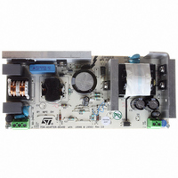
Manufacturer Part Number
EVL6566A-75WADP
Description
BOARD EVAL FOR L6566A
Manufacturer
STMicroelectronics
Type
Power Factor Correctionr
Datasheets
1.L6566ATR.pdf
(51 pages)
2.TSM1014IDT.pdf
(10 pages)
3.L6563ATR.pdf
(39 pages)
4.EVL6566A-75WADP.pdf
(8 pages)
Specifications of EVL6566A-75WADP
Main Purpose
AC/DC, Primary and Secondary Side with PFC
Outputs And Type
1, Isolated
Power - Output
75W
Voltage - Output
19V
Current - Output
4A
Voltage - Input
90 ~ 264VAC
Frequency - Switching
65kHz
Board Type
Fully Populated
Utilized Ic / Part
L6563, L6566A, TSM1014
Input Voltage
90 V to 264 V
Output Voltage
19 V
Dimensions
78 mm x 174 mm
Product
Power Management Modules
Lead Free Status / RoHS Status
Lead free / RoHS Compliant
Regulator Topology
-
Lead Free Status / Rohs Status
Lead free / RoHS Compliant
For Use With/related Products
L6563, L6566A
Other names
497-6449
Available stocks
Company
Part Number
Manufacturer
Quantity
Price


L6563 - L6563A
6.4
THD optimizer circuit
The L6563/A is provided with a special circuit that reduces the conduction dead-angle
occurring to the AC input current near the zero-crossings of the line voltage (crossover
distortion). In this way the THD (Total Harmonic Distortion) of the current is considerably
reduced.
A major cause of this distortion is the inability of the system to transfer energy effectively
when the instantaneous line voltage is very low. This effect is magnified by the high-
frequency filter capacitor placed after the bridge rectifier, which retains some residual
voltage that causes the diodes of the bridge rectifier to be reverse-biased and the input
current flow to temporarily stop.
To overcome this issue the device forces the PFC pre-regulator to process more energy
near the line voltage zero-crossings as compared to that commanded by the control loop.
This will result in both minimizing the time interval where energy transfer is lacking and fully
discharging the high-frequency filter capacitor after the bridge.
Figure 37 shows the internal block diagram of the THD optimizer circuit.
Figure 37. THD optimizer circuit
@ Vac1
@ Vac1
@ Vac2 > Vac1
@ Vac2 > Vac1
MULT
MULT
t
t
t
t
VFF
VFF
1 / V
1 / V
1 / V
GENERATOR
GENERATOR
GENERATOR
2
2
2
MULTIPLIER
MULTIPLIER
MULTIPLIER
OFFSET
OFFSET
OFFSET
COMP
COMP
t
t
+
+
+
+
t
t
comparator
comparator
Application information
to PWM
to PWM
t
t
t
t
21/39
Related parts for EVL6566A-75WADP
Image
Part Number
Description
Manufacturer
Datasheet
Request
R

Part Number:
Description:
BOARD DEMO FOR L6563/LL6566A
Manufacturer:
STMicroelectronics
Datasheet:

Part Number:
Description:
STMicroelectronics [RIPPLE-CARRY BINARY COUNTER/DIVIDERS]
Manufacturer:
STMicroelectronics
Datasheet:
Part Number:
Description:
STMicroelectronics [LIQUID-CRYSTAL DISPLAY DRIVERS]
Manufacturer:
STMicroelectronics
Datasheet:

Part Number:
Description:
BOARD EVAL FOR MEMS SENSORS
Manufacturer:
STMicroelectronics
Datasheet:
Part Number:
Description:
NPN TRANSISTOR POWER MODULE
Manufacturer:
STMicroelectronics
Datasheet:
Part Number:
Description:
TURBOSWITCH ULTRA-FAST HIGH VOLTAGE DIODE
Manufacturer:
STMicroelectronics
Datasheet:
Part Number:
Description:
Manufacturer:
STMicroelectronics
Datasheet:
Part Number:
Description:
DIODE / SCR MODULE
Manufacturer:
STMicroelectronics
Datasheet:
Part Number:
Description:
DIODE / SCR MODULE
Manufacturer:
STMicroelectronics
Datasheet:
Part Number:
Description:
Search -----> STE16N100
Manufacturer:
STMicroelectronics
Datasheet:
Part Number:
Description:
Search ---> STE53NA50
Manufacturer:
STMicroelectronics
Datasheet:
Part Number:
Description:
NPN Transistor Power Module
Manufacturer:
STMicroelectronics
Datasheet: