NCP1423EVB ON Semiconductor, NCP1423EVB Datasheet - Page 11
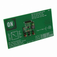
NCP1423EVB
Manufacturer Part Number
NCP1423EVB
Description
EVAL BOARD FOR NCP1423
Manufacturer
ON Semiconductor
Specifications of NCP1423EVB
Design Resources
NCP1423 Demo Board BOM NCP1423EVB Gerber Files NCP1423EVB Schematic
Main Purpose
DC/DC, Step Up
Outputs And Type
1, Non-Isolated
Voltage - Output
3.3V
Current - Output
400mA
Voltage - Input
2.5V
Regulator Topology
Boost
Frequency - Switching
600kHz
Board Type
Fully Populated
Utilized Ic / Part
NCP1423
Lead Free Status / RoHS Status
Lead free / RoHS Compliant
Power - Output
-
Lead Free Status / Rohs Status
Lead free / RoHS Compliant
For Use With/related Products
NCP1423
Other names
NCP1423EVBOS


IC is enabled again, and the internal circuit typically
consumes 9 mA of current from the OUT pin during normal
operation.
Low−Battery Detection
the low−battery detection function. When Pin 9 (LBI) is at
a voltage (defined by a resistor divider from the battery
voltage) lower than the internal reference voltage of 0.5 V,
the comparator output turns on a 50 W low side switch. It
pulls down the voltage at Pin 10 (LBO) which has hundreds
of kW of pull−high resistance. If the Pin 9 voltage is higher
than 0.5 V+15 mV, the comparator output turns off the 50 W
Output Voltage Setting
output voltage of the converter is determined by the external
feedback network comprised of R1 and R2 and the
relationship is given by:
where R1 and R2 are the upper and lower feedback resistors,
respectively.
Low Battery Detect Level Setting
determined by the external divider network comprised of R3
and R4 and the relationship is given by:
where R3 and R4 are the upper and lower divider resistors
respectively.
Inductor Selection
with a 5.6 mH inductor at V
supplying an output current up to 200 mA. For other input
/ output requirements, inductance in the range 3 mH to 10 mH
can be used according to end application specifications.
Selecting an inductor is a compromise between output
current capability, inductor saturation limit and tolerable
output voltage ripple. Low inductance values can supply
higher output current but also increase the ripple at output
and decrease efficiency. On the other hand, high inductance
values can improve output ripple and efficiency; however,
it also limited the output current capability at the same time.
This resistance can introduce unwanted power loss and
reduce overall efficiency. The basic rule is to select an
inductor with lowest DC resistance within the board space
limitation of the end application.
A comparator with 15 mV hysteresis is applied to perform
A typical application circuit is shown in Figure 1, The
The Low Battery Detect Voltage of the converter is
The NCP1423 is tested to produce optimum performance
Another parameter of the inductor is its DC resistance.
V OUT + 0.5 V
V LBI + 0.5 V
IN
= 1.3 V, V
1 ) R3
1 ) R1
R4
R2
APPLICATIONS INFORMATION
OUT
= 3.3 V,
http://onsemi.com
NCP1423
11
low side switch. When this occurs, Pin 10 becomes high
impedance and its voltage is pulled high again.
Auto Discharge
voltage status after the power down occur. This function is
using for communication with a digital signal. When auto
discharge function is enabled, the ADEN is set high; the
output capacitor will be discharged after the device is
shutdown. The capacitors connected to the output are
discharged by an integrated switch of 100 W. The residual
voltage on V
Capacitors Selection
the input and output terminals see impulsive voltage /
current waveforms. The currents flowing into and out of the
capacitors multiply with the Equivalent Series Resistance
(ESR) of the capacitor to produce ripple voltage at the
terminals. During the Syn−Rect switch−off cycle, the
charges stored in the output capacitor are used to sustain the
output load current. Load current at this period and the ESR
combined and reflect as ripple at the output terminals. For all
cases, the lower the capacitor ESR, the lower the ripple
voltage at output. As a general guideline, low ESR
capacitors should be used.
PCB Layout Recommendations
mode power conversion. Careful PCB layout can help to
minimize ground bounce, EMI noise, and unwanted
feedback that can affect the performance of the converter.
Hints suggested below can be used as a guideline in most
situations.
Grounding
output power return ground, the input power return ground,
and the device power ground together at one point. All
high−current paths must be as short as possible and thick
enough to allow current to flow through and produce
insignificant voltage drop along the path. The feedback
signal path must be separated from the main current path and
sense directly at the anode of the output capacitor.
Components Placement
output capacitor) must be placed as close together as
possible. All connecting traces must be short, direct and
thick. High current flowing and switching paths must be
kept away from the feedback (FB, Pin 3) terminal to avoid
unwanted injection of noise into the feedback path.
Auto discharge function is using for ensure the output
In all switching mode boost converter applications, both
Good PCB layout plays an important role in switching
A star−ground connection should be used to connect the
Power components (i.e. input capacitor, inductor and
OUT
will be less than 0.4 V after auto discharge.
Related parts for NCP1423EVB
Image
Part Number
Description
Manufacturer
Datasheet
Request
R

Part Number:
Description:
400 Ma Sync-rect Pfm Stepup Dcdc Converter With Truecutoff And Ringkiller
Manufacturer:
ON Semiconductor
Datasheet:
Part Number:
Description:
ON Semiconductor [VOLTAGE REGULATOR]
Manufacturer:
ON Semiconductor
Datasheet:
Part Number:
Description:
357-036-542-201 CARDEDGE 36POS DL .156 BLK LOPRO
Manufacturer:
ON Semiconductor
Datasheet:
Part Number:
Description:
357-036-542-201 CARDEDGE 36POS DL .156 BLK LOPRO
Manufacturer:
ON Semiconductor
Datasheet:
Part Number:
Description:
357-036-542-201 CARDEDGE 36POS DL .156 BLK LOPRO
Manufacturer:
ON Semiconductor
Datasheet:
Part Number:
Description:
357-036-542-201 CARDEDGE 36POS DL .156 BLK LOPRO
Manufacturer:
ON Semiconductor
Datasheet:
Part Number:
Description:
357-036-542-201 CARDEDGE 36POS DL .156 BLK LOPRO
Manufacturer:
ON Semiconductor
Datasheet:
Part Number:
Description:
357-036-542-201 CARDEDGE 36POS DL .156 BLK LOPRO
Manufacturer:
ON Semiconductor
Datasheet:
Part Number:
Description:
357-036-542-201 CARDEDGE 36POS DL .156 BLK LOPRO
Manufacturer:
ON Semiconductor
Datasheet:
Part Number:
Description:
357-036-542-201 CARDEDGE 36POS DL .156 BLK LOPRO
Manufacturer:
ON Semiconductor
Datasheet:
Part Number:
Description:
357-036-542-201 CARDEDGE 36POS DL .156 BLK LOPRO
Manufacturer:
ON Semiconductor
Datasheet:
Part Number:
Description:
357-036-542-201 CARDEDGE 36POS DL .156 BLK LOPRO
Manufacturer:
ON Semiconductor
Datasheet:
Part Number:
Description:
Manufacturer:
ON Semiconductor
Datasheet:
Part Number:
Description:
Manufacturer:
ON Semiconductor
Datasheet: