NCP1423EVB ON Semiconductor, NCP1423EVB Datasheet - Page 8
NCP1423EVB
Manufacturer Part Number
NCP1423EVB
Description
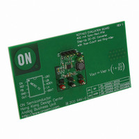
EVAL BOARD FOR NCP1423
Manufacturer
ON Semiconductor
Specifications of NCP1423EVB
Design Resources
NCP1423 Demo Board BOM NCP1423EVB Gerber Files NCP1423EVB Schematic
Main Purpose
DC/DC, Step Up
Outputs And Type
1, Non-Isolated
Voltage - Output
3.3V
Current - Output
400mA
Voltage - Input
2.5V
Regulator Topology
Boost
Frequency - Switching
600kHz
Board Type
Fully Populated
Utilized Ic / Part
NCP1423
Lead Free Status / RoHS Status
Lead free / RoHS Compliant
Power - Output
-
Lead Free Status / Rohs Status
Lead free / RoHS Compliant
For Use With/related Products
NCP1423
Other names
NCP1423EVBOS


250
200
150
100
50
Upper Trace: Output Voltage Ripple, 100 mV/Division
Middle Trace: Voltage at Lx pin, 2.0 V/Division
Lower Trace: Inductor Current, 500 mA/Division
(V
0
Figure 21. Output Ripple Voltage vs. Battery Input
1.3
Figure 25. Discontinuous Conduction Mode
IN
Upper Trace: Voltage at LBI Pin, 0.5 V/Division
Lower Trace: Voltage at LBO Pin, 1.0 V/Division
V
C
T
= 1.5 V, V
A
OUT
IN
= 25°C
= 10 mF, C
= 3.3 V, L = 5.6 mH
1.5
V
OUT
Figure 23. Low Battery Detect
BATT
Switching Waveform
= 3.3 V, I
, BATTERY INPUT VOLTAGE (V)
OUT
1.7
= 22 mF
LOAD
Voltage
= 50 mA; L = 5.6 mH, C
1.9
TYPICAL OPERATING CHARACTERISTICS
2.1
50 mA
2.3
OUT
100 mA
http://onsemi.com
= 22 mF)
NCP1423
2.5
8
12.5
7.5
5.0
2.5
15
10
Upper Trace: Output Voltage Ripple, 100 mV/Division
Middle Trace: Voltage at LX pin, 2.0 V/Division
Lower Trace: Inductor Current, 500 mA/Division
(V
1.8
IN
Upper Trace: Output Voltage Waveform, 2.0 V/Division
Middle Trace: Input Voltage Waveform, 1.0 V/Division
Lower Trace: Inductor Current Waveform, 500 mA/Division
(V
IN
= 1.5 V, V
Figure 22. No Load Operating Current vs. Input
Figure 26. Continuous Conduction Mode
= 1.8 V, V
Figure 24. Startup Transient Response
V
2.1
OUT
OUT
OUT
, INPUT VOLTAGE AT OUT PIN (V)
= 3.3 V, I
Switching Waveform
= 3.3 V, L = 5.6 mH, I
Voltage at OUT Pin
2.4
LOAD
= 200 mA; L = 5.6 mH, C
L = 5.6 mH, C
C
OUT
2.7
LOAD
= 22 mF, T
= 60 mA)
IN
3.0
= 10 mF,
A
= 25°C
OUT
= 22 mF)
3.3
Related parts for NCP1423EVB
Image
Part Number
Description
Manufacturer
Datasheet
Request
R

Part Number:
Description:
400 Ma Sync-rect Pfm Stepup Dcdc Converter With Truecutoff And Ringkiller
Manufacturer:
ON Semiconductor
Datasheet:
Part Number:
Description:
ON Semiconductor [VOLTAGE REGULATOR]
Manufacturer:
ON Semiconductor
Datasheet:
Part Number:
Description:
357-036-542-201 CARDEDGE 36POS DL .156 BLK LOPRO
Manufacturer:
ON Semiconductor
Datasheet:
Part Number:
Description:
357-036-542-201 CARDEDGE 36POS DL .156 BLK LOPRO
Manufacturer:
ON Semiconductor
Datasheet:
Part Number:
Description:
357-036-542-201 CARDEDGE 36POS DL .156 BLK LOPRO
Manufacturer:
ON Semiconductor
Datasheet:
Part Number:
Description:
357-036-542-201 CARDEDGE 36POS DL .156 BLK LOPRO
Manufacturer:
ON Semiconductor
Datasheet:
Part Number:
Description:
357-036-542-201 CARDEDGE 36POS DL .156 BLK LOPRO
Manufacturer:
ON Semiconductor
Datasheet:
Part Number:
Description:
357-036-542-201 CARDEDGE 36POS DL .156 BLK LOPRO
Manufacturer:
ON Semiconductor
Datasheet:
Part Number:
Description:
357-036-542-201 CARDEDGE 36POS DL .156 BLK LOPRO
Manufacturer:
ON Semiconductor
Datasheet:
Part Number:
Description:
357-036-542-201 CARDEDGE 36POS DL .156 BLK LOPRO
Manufacturer:
ON Semiconductor
Datasheet:
Part Number:
Description:
357-036-542-201 CARDEDGE 36POS DL .156 BLK LOPRO
Manufacturer:
ON Semiconductor
Datasheet:
Part Number:
Description:
357-036-542-201 CARDEDGE 36POS DL .156 BLK LOPRO
Manufacturer:
ON Semiconductor
Datasheet:
Part Number:
Description:
Manufacturer:
ON Semiconductor
Datasheet:
Part Number:
Description:
Manufacturer:
ON Semiconductor
Datasheet: