NCP1423EVB ON Semiconductor, NCP1423EVB Datasheet - Page 2
NCP1423EVB
Manufacturer Part Number
NCP1423EVB
Description
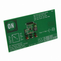
EVAL BOARD FOR NCP1423
Manufacturer
ON Semiconductor
Specifications of NCP1423EVB
Design Resources
NCP1423 Demo Board BOM NCP1423EVB Gerber Files NCP1423EVB Schematic
Main Purpose
DC/DC, Step Up
Outputs And Type
1, Non-Isolated
Voltage - Output
3.3V
Current - Output
400mA
Voltage - Input
2.5V
Regulator Topology
Boost
Frequency - Switching
600kHz
Board Type
Fully Populated
Utilized Ic / Part
NCP1423
Lead Free Status / RoHS Status
Lead free / RoHS Compliant
Power - Output
-
Lead Free Status / Rohs Status
Lead free / RoHS Compliant
For Use With/related Products
NCP1423
Other names
NCP1423EVBOS


Stresses exceeding Maximum Ratings may damage the device. Maximum Ratings are stress ratings only. Functional operation above the
Recommended Operating Conditions is not implied. Extended exposure to stresses above the Recommended Operating Conditions may affect
device reliability.
NOTE: ESD data available upon request.
1. This device contains ESD protection and exceeds the following tests:
2. The maximum package power dissipation limit must not be exceeded.
3. Latchup Current Maximum Rating: ±150 mA per JEDEC standard: JESD78.
4. Moisture Sensitivity Level: MSL 1 per IPC/JEDEC standard: J−STD−020A.
5. Measured on approximately 1 in sq of 1 oz Cu.
PIN DESCRIPTION
MAXIMUM RATINGS
Power Supply (Pin 6)
Input / Output Pins (Pins 1−3,5,7−10)
Thermal Characteristics
Micro10 Plastic Package, Case 846B, T
Thermal Resistance Junction−to−Air
Operating Junction Temperature Range
Operating Ambient Temperature Range
Storage Temperature Range
Pin No.
10
1
2
3
4
5
6
7
8
9
Human Body Model (HBM) ±2.0 kV per JEDEC standard: JESD22−A114.
Machine Model (MM) ±200 V per JEDEC standard: JESD22−A115.
0.1 mF
Symbol
ADEN
GND
OUT
REF
LBO
BAT
LBI
EN
FB
LX
P D +
R1
R2
22 mF
C
OUT
C1
T J(max) * T A
ON
OFF
Low−Battery Detector Input and Enable. With this pin pulled down below 0.5 V, the device will be disabled
and will enter shutdown mode
1.195 V Reference Voltage Output, bypass with 0.1 mF capacitor if this pin is not loaded, with a 1.0 mF
bypassing capacitor, this pin can be loaded up to 2.5 mA @ V
Output Voltage Feedback Input
Ground
Power Output. OUT provides bootstrap power to the IC
Battery supply input pin and connection for internal Ring−Killer
N−Channel and P−Channel Power MOSFET Drain
Auto Discharge Input
Low−Battery Detector Input
Open−Drain Low−Battery Detector Output. Output is Low when V
LBO is high impedance shutdown
*
R qJA
Rating
A
= 25°C
* Optional
EN
REF
FB
GND
OUT
Figure 1. Typical Operation Circuit
NCP1423
http://onsemi.com
ADEN
NCP1423
LBO
BAT
LBI
LX
100k
2
Description
5.6 mH
10 mF
ON
OFF
C
IN
Symbol
V
R
T
V
P
OUT
T
T
qJA
stg
IO
A
D
J
OUT
LBI
R4
= 3.3 V.
is < 500 mV.
R3
− 40 to + 150
− 55 to +150
− 40 to + 85
−0.3, 6.0
−0.3, 6.0
Value
480
250
Low battery
open drain output
Low battery
sense input
°C/W
Unit
mW
°C
°C
°C
V
V
Related parts for NCP1423EVB
Image
Part Number
Description
Manufacturer
Datasheet
Request
R

Part Number:
Description:
400 Ma Sync-rect Pfm Stepup Dcdc Converter With Truecutoff And Ringkiller
Manufacturer:
ON Semiconductor
Datasheet:
Part Number:
Description:
ON Semiconductor [VOLTAGE REGULATOR]
Manufacturer:
ON Semiconductor
Datasheet:
Part Number:
Description:
357-036-542-201 CARDEDGE 36POS DL .156 BLK LOPRO
Manufacturer:
ON Semiconductor
Datasheet:
Part Number:
Description:
357-036-542-201 CARDEDGE 36POS DL .156 BLK LOPRO
Manufacturer:
ON Semiconductor
Datasheet:
Part Number:
Description:
357-036-542-201 CARDEDGE 36POS DL .156 BLK LOPRO
Manufacturer:
ON Semiconductor
Datasheet:
Part Number:
Description:
357-036-542-201 CARDEDGE 36POS DL .156 BLK LOPRO
Manufacturer:
ON Semiconductor
Datasheet:
Part Number:
Description:
357-036-542-201 CARDEDGE 36POS DL .156 BLK LOPRO
Manufacturer:
ON Semiconductor
Datasheet:
Part Number:
Description:
357-036-542-201 CARDEDGE 36POS DL .156 BLK LOPRO
Manufacturer:
ON Semiconductor
Datasheet:
Part Number:
Description:
357-036-542-201 CARDEDGE 36POS DL .156 BLK LOPRO
Manufacturer:
ON Semiconductor
Datasheet:
Part Number:
Description:
357-036-542-201 CARDEDGE 36POS DL .156 BLK LOPRO
Manufacturer:
ON Semiconductor
Datasheet:
Part Number:
Description:
357-036-542-201 CARDEDGE 36POS DL .156 BLK LOPRO
Manufacturer:
ON Semiconductor
Datasheet:
Part Number:
Description:
357-036-542-201 CARDEDGE 36POS DL .156 BLK LOPRO
Manufacturer:
ON Semiconductor
Datasheet:
Part Number:
Description:
Manufacturer:
ON Semiconductor
Datasheet:
Part Number:
Description:
Manufacturer:
ON Semiconductor
Datasheet: