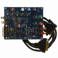
CDB4351 Cirrus Logic Inc, CDB4351 Datasheet - Page 20

CDB4351
Manufacturer Part Number
CDB4351
Description
BOARD EVAL FOR CS4351 DAC
Manufacturer
Cirrus Logic Inc
Series
Popguard®r
Specifications of CDB4351
Number Of Dac's
2
Number Of Bits
24
Outputs And Type
1, Single Ended
Sampling Rate (per Second)
192k
Data Interface
Serial
Dac Type
Voltage
Voltage Supply Source
Analog and Digital
Operating Temperature
-10°C ~ 70°C
Utilized Ic / Part
CS4351
Description/function
Audio D/A
Operating Supply Voltage
5 V
Product
Audio Modules
For Use With/related Products
CS4351
Lead Free Status / RoHS Status
Contains lead / RoHS non-compliant
Lead Free Status / RoHS Status
Lead free / RoHS Compliant, Contains lead / RoHS non-compliant
Other names
598-1152
20
4.9
4.9.1
4.9.2
Control Port Interface
The control port is used to load all the internal register settings (see
port may be completely asynchronous with the audio sample rate. However, to avoid potential interference
problems, the control port pins should remain static if no operation is required.
The control port operates in one of two modes: I²C or SPI.
4.9.2.1
To write to the device, follow the procedure below while adhering to the control port Switching Specifica-
tions in
MAP Auto Increment
The device has MAP (memory address pointer) auto increment capability enabled by the INCR bit (also
the MSB) of the MAP. If INCR is set to 0, MAP will stay constant for successive I²C writes or reads and
SPI writes. If INCR is set to 1, MAP will auto increment after each byte is written, allowing block reads or
writes of successive registers.
I²C Mode
In the I²C mode, data is clocked into and out of the bi-directional serial control data line, SDA, by the serial
control port clock, SCL (see
ables the user to alter the chip address (100110[AD0][R/W]) and should be tied to VL or GND as required,
before powering up the device. If the device ever detects a high to low transition on the AD0/CS pin after
power-up, SPI mode will be selected.
1. Initiate a START condition to the I²C bus followed by the address byte. The upper 6 bits must be
2. Wait for an acknowledge (ACK) from the part, then write to the memory address pointer, MAP. This
3. Wait for an acknowledge (ACK) from the part, then write the desired data to the register pointed to
4. If the INCR bit (see
5. If the INCR bit is set to 0 and further I²C writes to other registers are desired, it is necessary to initiate
100110. The seventh bit must match the setting of the AD0 pin, and the eighth must be 0. The eighth
bit of the address byte is the R/W bit.
byte points to the register to be written.
by the MAP.
are written, then initiate a STOP condition to the bus.
a repeated START condition and follow the procedure detailed from step 1. If no further writes to oth-
er registers are desired, initiate a STOP condition to the bus.
Section
I²C Write
8.
Section
Figure 9
4.9.1) is set to 1, repeat the previous step until all the desired registers
for the clock to data relationship). There is no CS pin. Pin AD0 en-
Section
6). The operation of the control
CS4351
DS566F1


