CDB4385 Cirrus Logic Inc, CDB4385 Datasheet
CDB4385
Specifications of CDB4385


Related parts for CDB4385


CDB4385 Summary of contents
Page 1
... The CS4385 is available in a 48-pin LQFP package in both Commercial (-40°C to +85°C) and Automotive (-40°C to +105°C) grades. The CDB4385 Customer Demonstration board is also available for device evalu- ation and implementation suggestions. Please see “ ...
Page 2
TABLE OF CONTENTS 1. PIN DESCRIPTION 2. CHARACTERISTICS AND SPECIFICATIONS ...................................................................................... 8 RECOMMENDED OPERATING CONDITIONS ..................................................................................... 8 ABSOLUTE MAXIMUM RATINGS ......................................................................................................... 8 DAC ANALOG CHARACTERISTICS - COMMERCIAL (-CQZ) ............................................................. 9 DAC ANALOG CHARACTERISTICS - AUTOMOTIVE (-DQZ) ............................................................ 10 POWER AND ...
Page 3
Mode Control 1 (address 02h) ........................................................................................................ 37 6.2.1 Control Port Enable (CPEN) .................................................................................................. 37 6.2.2 Freeze Controls (FREEZE) ................................................................................................... 37 6.2.3 PCM/DSD Selection (DSD/PCM) .......................................................................................... 38 6.2.4 DAC Pair Disable (DACx_DIS) .............................................................................................. 38 6.2.5 Power Down (PDN) ............................................................................................................... 38 ...
Page 4
LIST OF FIGURES Figure 1.Serial Audio Interface Timing ...................................................................................................... 15 Figure 2.TDM Serial Audio Interface Timing ............................................................................................. 15 Figure 3.Direct Stream Digital - Serial Audio Input Timing ........................................................................ 16 Figure 4.Direct Stream Digital - Serial Audio Input Timing for Phase ...
Page 5
LIST OF TABLES Table 1. Single-Speed Mode Standard Frequencies ................................................................................ 21 Table 2. Double-Speed Mode Standard Frequencies ............................................................................... 21 Table 3. Quad-Speed Mode Standard Frequencies ................................................................................. 21 Table 4. PCM Digital Interface Format, Hardware Mode Options ............................................................. 22 Table 5. ...
Page 6
PIN DESCRIPTION DSDA2 DSDB1 DSDA1 MCLK LRCK SDIN1 SCLK M4(TST) SDIN2 M3(TST) Pin Name # Digital Power (Input) - Positive power supply for the digital section. Refer to the Recommended Oper ating Conditions for appropriate voltages. 5 ...
Page 7
Pin Name # AOUTA1 +,- 39, 40 AOUTB1 +,- 38, 37 AOUTA2 +,- 35, 36 AOUTB2 +,- 34, 33 Differential Analog Output (Output) - The full-scale differential analog output level is specified in the AOUTA3 +,- 29, 30 Analog Characteristics ...
Page 8
CHARACTERISTICS AND SPECIFICATIONS RECOMMENDED OPERATING CONDITIONS GND = 0 V; all voltages with respect to ground. Parameters DC Power Supply Ambient Operating Temperature (Power Applied) ABSOLUTE MAXIMUM RATINGS GND = 0 V; all voltages with respect to ground. Parameters ...
Page 9
DAC ANALOG CHARACTERISTICS - COMMERCIAL (-CQZ) Test Conditions (unless otherwise specified VLS = VLC = 2 input sine wave ; Tested under max ac-load resistance (Note 1) “Typical Connection Diagram” on page ...
Page 10
DAC ANALOG CHARACTERISTICS - AUTOMOTIVE (-DQZ) Test Conditions (unless otherwise specified 4.75 to 5.25 V; VLS = 1.71 to 5.25 V; VLC = 1. 2. -40°C to 85°C; ...
Page 11
POWER AND THERMAL CHARACTERISTICS Parameters Power Supplies Power Supply Current (Note 4) (Note 5) (Note 6) Power Dissipation (Note 4) Package Thermal Resistance Power Supply Rejection Ratio (Note 7) Notes: 4. Current consumption increases with increasing Fs within a given ...
Page 12
COMBINED INTERPOLATION & ON-CHIP ANALOG FILTER RESPONSE The filter characteristics have been normalized to the sample rate (Fs) and can be referenced to the desired sam- ple rate by multiplying the given characteristic by Fs. See Parameter Combined Digital and ...
Page 13
COMBINED INTERPOLATION & ON-CHIP ANALOG FILTER RESPONSE (CONTINUED) Parameter Single-Speed Mode - 48 kHz Passband (Note 9) Frequency Response StopBand StopBand Attenuation Group Delay De-emphasis Error (Note 11) (Relative to 1 kHz) Double-Speed Mode - 96 kHz Passband (Note 9) ...
Page 14
DIGITAL CHARACTERISTICS Parameters Input Leakage Current Input Capacitance High-Level Input Voltage Low-Level Input Voltage Low-Level Output Voltage (I = -1.2 mA) OL Low-Level Output Voltage (I = -1.2 mA) Control I/O = 1 MUTEC auto detect ...
Page 15
SWITCHING CHARACTERISTICS - PCM Inputs: Logic 0 = GND, Logic 1 = VLS, C Parameters RST pin Low Pulse Width MCLK Frequency MCLK Duty Cycle Input Sample Rate - LRCK (Manual selection) Input Sample Rate - LRCK (Auto detect) LRCK ...
Page 16
SWITCHING CHARACTERISTICS - DSD Logic 0 = GND; Logic 1 = VLS Parameter MCLK Duty Cycle DSD_SCLK Pulse Width Low DSD_SCLK Pulse Width High DSD_SCLK Frequency DSD_A / _B valid to DSD_SCLK rising setup time DSD_SCLK rising to ...
Page 17
SWITCHING CHARACTERISTICS - CONTROL PORT - I²C FORMAT Inputs: Logic 0 = GND, Logic 1 = VLC, C Parameter SCL Clock Frequency RST Rising Edge to Start Bus Free Time Between Transmissions Start Condition Hold Time (prior to first clock ...
Page 18
SWITCHING CHARACTERISTICS - CONTROL PORT - SPI FORMAT Inputs: Logic 0 = GND, Logic 1 = VLC, C Parameter CCLK Clock Frequency RST Rising Edge to CS Falling CCLK Edge to CS Falling CS High Time Between Transmissions CS Falling ...
Page 19
TYPICAL CONNECTION DIAGRAM +2.5 V PCM Digital Audio Source +1 DSD Audio Source Micro- Controller +1 Note: Necessary for I control port operation Figure 7. Typical Connection Diagram, Software Mode DS671F2 ...
Page 20
V PCM Digital Audio Source +1 DSD Audio Source Stand-Alone Mode Configuration +1 Figure 8. Typical Connection Diagram, Hardware µF 0.1 µ AOUTA1+ AOUTA1- ...
Page 21
APPLICATIONS The CS4385 serially accepts two’s complement formatted PCM data at standard audio sample rates including 48, 44.1 and 32 kHz in SSM, 96, 88.2 and 64 kHz in DSM, and 192, 176.4 and 128 kHz in QSM. Audio ...
Page 22
Mode Select In Hardware Mode, operation is determined by the Mode Select pins. The states of these pins are continu- ally scanned for any changes; however, the mode should only be changed while the device is in reset (RST ...
Page 23
Digital Interface Formats The serial port operates as a slave and supports the I²S, Left-Justified, Right-Justified, One-Line Mode (OLM) and TDM digital interface formats with varying bit depths from 16 to 32, as shown in Data is clocked into ...
Page 24
LRCK SCLK SDINx Figure 14. Format 5 - Right-Justified 18-bit Data 4.3.1 OLM #1 OLM #1 serial audio interface format operates in Single-, Double-, or Quad-Speed Mode and will slave ...
Page 25
OLM #3 OLM #3 serial audio interface format operates in Single-, Double-, or Quad-Speed Mode and will slave to SCLK at 256 Fs. Eight channels of MSB first 20-bit PCM data are input on SDIN1. 128 clks LRCK Left ...
Page 26
TDM The TDM serial audio interface format operates in Single-, Double-, or Quad-Speed Mode and will slave to SCLK at 256 Fs. Data is received most significant bit first on the first SCLK after an LRCK transition and is ...
Page 27
De-Emphasis The CS4385 includes on-chip digital de-emphasis filters. The de-emphasis feature is included to accommo- date older audio recordings that utilize pre-emphasis equalization as a means of noise reduction. shows the de-emphasis curve. The frequency response of the de-emphasis ...
Page 28
Direct Stream Digital (DSD) Mode In Software Mode, the DSD/PCM bits (Reg. 02h) are used to configure the device for DSD Mode. The DSD_DIF bits (Reg 04h) then control the expected DSD rate and MCLK ratio. The DIR_DSD bit ...
Page 29
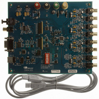
... DAC. If desired, all supply pins with similar voltage ratings may be connected to the same supply, but a decoupling capacitor should still be placed on each supply pin. Notes: All decoupling capacitors should be referenced to ground. The CDB4385 evaluation board demonstrates the optimum layout and power supply arrangements. 4.10 Analog Output and Filtering The application note “ ...
Page 30
The MUTEC Outputs The MUTEC1 and MUTEC234 pins have an auto-polarity detect feature. The MUTEC output pins are high impedance at the time of reset. The external mute circuitry needs to be self-biased into an active state in order ...
Page 31
Recommended Power-Up Sequence 4.12.1 Hardware Mode 1. Hold RST low until the power supplies and configuration pins are stable, and the master and left/right clocks are locked to the appropriate frequencies, as discussed in registers are reset to the ...
Page 32
Software Mode 1. Hold RST low until the power supply is stable, and the master and left/right clocks are locked to the appropriate frequencies, as discussed in settings, FILT+ will remain low, and VQ will be connected to VA/2. ...
Page 33
I²C Write To write to the device, follow the procedure below while adhering to the control port Switching Specifica- tions in Section 1. 1. Initiate a START condition to the I²C bus followed by the address byte. The upper ...
Page 34
SPI Mode In SPI Mode, data is clocked into the serial control data line, CDIN, by the serial control port clock, CCLK (see Figure 27 for the clock to data relationship). There is no AD0 pin. Pin CS is ...
Page 35
REGISTER QUICK REFERENCE Addr Function 7 01h Chip Revision PART4 default 0 02h Mode Control CPEN default 0 03h PCM Control DIF3 default 0 04h DSD Control DSD_DIF2 DSD_DIF1 DSD_DIF0 DIR_DSD STATIC_D default 0 05h Filter Control Reserved default ...
Page 36
Addr Function 7 14h Vol. Control A4 A4_VOL7 default 0 15h Vol. Control B4 B4_VOL7 default 0 16h PCM clock mode Reserved default A4_VOL6 A4_VOL5 A4_VOL4 A4_VOL3 B4_VOL6 B4_VOL5 B4_VOL4 B4_VOL3 0 ...
Page 37
REGISTER DESCRIPTION Note: All registers are read/write in I²C Mode and write only in SPI, unless otherwise noted. 6.1 Chip Revision (address 01h PART4 PART3 PART2 0 0 6.1.1 Part Number ID (PART) [Read Only] 00001- CS4385 ...
Page 38
PCM/DSD Selection (DSD/PCM) Default = PCM 1 - DSD Function: This function selects DSD or PCM Mode. The appropriate data and clocks should be present before changing modes, or else MUTE should be selected. 6.2.4 DAC ...
Page 39
DIF3 DIF2 DIF1 6.3.2 ...
Page 40
Direct DSD Conversion (DIR_DSD) Function: When set to 0 (default), DSD input data is sent to the DSD processor for filtering and volume control func- tions. When set to 1, DSD input data is sent directly to the switched ...
Page 41
Filter Control (address 05h Reserved Reserved Reserved 0 0 6.5.1 Interpolation Filter Select (FILT_SEL) Function: When set to 0 (default), the Interpolation Filter has a fast roll-off. When set to 1, the Interpolation Filter has a slow ...
Page 42
Channel A Volume = Channel B Volume (Px_A=B) Default = Disabled 1 - Enabled Function: The AOUTAx and AOUTBx volume levels are independently controlled by the A and the B Channel Vol- ume Control Bytes when ...
Page 43
Soft Ramp on Zero Crossing Soft Ramp and Zero Cross Enable dictates that signal-level changes, either by attenuation changes or muting, will occur in 1/8 dB steps and be implemented on a signal zero crossing. The 1/8 dB level change ...
Page 44
DSD Auto-Mute (DAMUTE) Function: When set to 1 (default), the Digital-to-Analog converter output will mute following the reception of 256 re- peated 8-bit DSD mute patterns (as defined in the SACD specification). A single bit not fitting the repeated ...
Page 45
Mixing Control (address 0Ah, 0Dh, 10h, 13h Reserved Px_DEM1 Px_DEM0 0 0 6.10.1 De-Emphasis Control (PX_DEM1:0) Default = Disabled 01 - 44.1 kHz kHz kHz Function: Selects the ...
Page 46
ATAPI4 ATAPI3 ATAPI2 6.11 Volume Control (address 0Bh, 0Ch, 0Eh, 0Fh, 11h, 12h, 14h, ...
Page 47
PCM Clock Mode (address 16h Reserved Reserved MCLKDIV 0 0 6.12.1 Master Clock DIVIDE by 2 ENABLE (MCLKDIV) Function: When set to 1, the MCLKDIV bit enables a circuit which divides the externally applied MCLK signal by ...
Page 48
FILTER PLOTS 0 −20 −40 −60 −80 −100 −120 0.4 0.5 0.6 0.7 Frequency(normalized to Fs) Figure 28. Single-Speed (fast) Stopband Rejection 0 −1 −2 −3 −4 −5 −6 −7 −8 −9 −10 0.45 0.46 0.47 0.48 0.49 0.5 ...
Page 49
Frequency(normalized to Fs) Figure 34. Single-Speed (slow) Transition Band (detail 100 120 0.4 0.5 0.6 0.7 Frequency(normalized ...
Page 50
Frequency(normalized to Fs) Figure 40. Double-Speed (slow) Stopband Rejection 0.45 0.46 0.47 0.48 0.49 0.5 0.51 Frequency(normalized ...
Page 51
Frequency(normalized to Fs) Figure 46. Quad-Speed (fast) Transition Band (detail 100 120 0.1 0.2 0.3 0.4 0.5 ...
Page 52
PARAMETER DEFINITIONS Total Harmonic Distortion + Noise (THD+N) The ratio of the rms value of the signal to the rms sum of all other spectral components over the specified bandwidth (typically kHz), including distortion components. ...
Page 53
PACKAGE DIMENSIONS 48L LQFP PACKAGE DRAWING D D1 DIM MIN A --- A1 0.002 B 0.007 D 0.343 D1 0.272 E 0.343 E1 0.272 e* 0.016 L 0.018 µ 0.000° DS671F2 ∝ L INCHES ...
Page 54
... How to Achieve Optimum Performance from Delta-Sigma A/D & D/A Converters, by Steven Harris. Paper presented at the 93rd Convention of the Audio Engineering Society, October 1992. 2. CDB4385 data sheet, available at http://www.cirrus.com. 3. Design Notes for a 2-Pole Filter with Differential Input, by Steven Green. Cirrus Logic Application Note AN48 4. The I² ...
Page 55
Contacting Cirrus Logic Support For all product questions and inquiries, contact a Cirrus Logic Sales Representative. To find the one nearest to you IMPORTANT NOTICE Cirrus Logic, Inc. and its subsidiaries ("Cirrus") believe that the information contained in ...