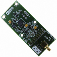
EVAL-AD5443-DBRDZ Analog Devices Inc, EVAL-AD5443-DBRDZ Datasheet - Page 20

EVAL-AD5443-DBRDZ
Manufacturer Part Number
EVAL-AD5443-DBRDZ
Description
BOARD EVAL CARD CLINUX/STAMP
Manufacturer
Analog Devices Inc
Datasheet
1.AD5443YRMZ.pdf
(28 pages)
Specifications of EVAL-AD5443-DBRDZ
Number Of Dac's
1
Number Of Bits
12
Outputs And Type
1, Differential
Sampling Rate (per Second)
2.5M
Data Interface
Serial
Settling Time
50ns
Dac Type
Current
Voltage Supply Source
Single
Operating Temperature
-40°C ~ 125°C
Utilized Ic / Part
AD5443
Silicon Manufacturer
Analog Devices
Application Sub Type
DAC
Kit Application Type
Data Converter
Silicon Core Number
AD5443
Kit Contents
Board
Development Tool Type
Hardware - Eval/Demo Board
Rohs Compliant
Yes
Lead Free Status / RoHS Status
Lead free / RoHS Compliant
AD5426/AD5432/AD5443
SERIAL INTERFACE
The AD5426/AD5432/AD5443 have an easy to use 3-wire inter-
face that is compatible with SPI/QSPI/MICROWIRE and DSP
interface standards. Data is written to the device in 16 bit words.
This 16-bit word consists of 4 control bits and either 8 , 10 , or 12
data bits as shown in Figure 48, Figure 49, and Figure 50. The
AD5443 uses all 12 bits of DAC data. The AD5432 uses 10 bits
and ignores the 2 LSBs, while the AD5426 uses 8 bits and ignores
the last 4 bits.
Low Power Serial Interface
To minimize the power consumption of the device, the interface
powers up fully only when the device is being written to, that is,
on the falling edge of SYNC . The SCLK and DIN input buffers
are powered down on the rising edge of SYNC . The SYNC of
the AD5426/AD5432/AD5443 needs to be synchronous with
the microprocessor control. Unfinished data frames are latched
into the part and will affect the output.
DAC Control Bits C3 to C0
Control Bits C3 to C0 allow control of various functions of
the DAC, as seen in Table 10. Default settings of the DAC on
power-on are as follows: Data is clocked into the shift register
on falling clock edges and daisy-chain mode is enabled.
Device powers on with zero-scale load to the DAC register
and I
The DAC control bits allow the user to adjust certain features
on power-on, for example, daisy-chaining may be disabled if
not in use, active clock edge may be changed to rising edge, and
DAC output may be cleared to either zero scale or midscale.
The user may also initiate a readback of the DAC register
contents for verification purposes.
Table 10. DAC Control Bits
C3
0
0
0
0
0
0
0
0
1
1
1
1
1
1
1
1
OUT
C2
0
0
0
0
1
1
1
1
0
0
0
0
1
1
1
1
lines.
C1
0
0
1
1
0
0
1
1
0
0
1
1
0
0
1
1
C0
0
1
0
1
0
1
0
1
0
1
0
1
0
1
0
1
Function Implemented
No operation (power-on default)
Load and update
Initiate readback
Reserved
Reserved
Reserved
Reserved
Reserved
Reserved
Daisy-chain disable
Clock data to shift register on rising edge
Clear DAC output to zero scale
Clear DAC output to midscale
Reserved
Reserved
Reserved
Rev. C | Page 20 of 28
SYNC Function
SYNC is an edge-triggered input that acts as a frame synchro-
nization signal and chip enable. Data can be transferred into the
device only while SYNC is low. To start the serial data transfer,
SYNC should be taken low observing the minimum SYNC
falling to SCLK falling edge setup time, t
Daisy-Chain Mode
Daisy-chain is the default power-on mode. To disable the daisy
chain function, write 1001 to the control word. In daisy-chain
mode, the internal gating on SCLK is disabled. The SCLK is
continuously applied to the input shift register when SYNC is
low. If more than 16 clock pulses are applied, the data ripples
out of the shift register and appears on the SDO line. This data
is clocked out on the rising edge of SCLK (this is the default, use
the control word to change the active edge) and is valid for the
next device on the falling edge (default). By connecting this line
to the D
interface is constructed. Sixteen clock pulses are required for
each device in the system. Therefore, the total number of clock
cycles must equal 16 N where N is the total number of devices
in the chain. See the timing diagram in
When the serial transfer to all devices is complete, SYNC
should be taken high. This prevents any further data being
clocked into the input shift register. A burst clock containing
the exact number of clock cycles may be used and SYNC taken
high some time later. After the rising edge of SYNC , data is
automatically transferred from each device’s input shift register
to the addressed DAC.
When control bits = 0000, the device is in no operation mode.
This may be useful in daisy-chain applications where the user
does not want to change the settings of a particular DAC in the
chain. Simply write 0000 to the control bits for that DAC and
the following data bits will be ignored. To re-enable the daisy-
chain mode, if disabled, a power recycle is required.
DB15 (MSB)
DB15 (MSB)
DB15 (MSB)
C3
C3
C3
CONTROL BITS
CONTROL BITS
CONTROL BITS
C2
C2
C2
IN
C1
C1
C1
Figure 49. AD5432 10-Bit Input Shift Register Contents
Figure 50. AD5443 12-Bit Input Shift Register Contents
Figure 48. AD5426 8-Bit Input Shift Register Contents
input on the next device in the chain, a multidevice
C0
C0
C0 DB11 DB10
DB7 DB6 DB5 DB4 DB3 DB2
DB9
DB8
DB7 DB6
DB9
DB8
DB5 DB4 DB3 DB2
DB7 DB6 DB5 DB4 DB3 DB2
DATA BITS
DATA BITS
DATA BITS
DB1
Figure 4
4
.
DB0
DB1
X
.
DB0
X
DB0 (LSB)
DB1
X
DB0 (LSB)
DB0 (LSB)
X
DB0
X
X


