EVAL-AD5443-DBRDZ Analog Devices Inc, EVAL-AD5443-DBRDZ Datasheet - Page 7
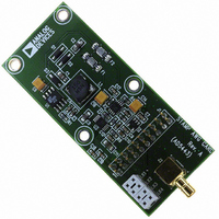
EVAL-AD5443-DBRDZ
Manufacturer Part Number
EVAL-AD5443-DBRDZ
Description
BOARD EVAL CARD CLINUX/STAMP
Manufacturer
Analog Devices Inc
Datasheet
1.AD5443YRMZ.pdf
(28 pages)
Specifications of EVAL-AD5443-DBRDZ
Number Of Dac's
1
Number Of Bits
12
Outputs And Type
1, Differential
Sampling Rate (per Second)
2.5M
Data Interface
Serial
Settling Time
50ns
Dac Type
Current
Voltage Supply Source
Single
Operating Temperature
-40°C ~ 125°C
Utilized Ic / Part
AD5443
Silicon Manufacturer
Analog Devices
Application Sub Type
DAC
Kit Application Type
Data Converter
Silicon Core Number
AD5443
Kit Contents
Board
Development Tool Type
Hardware - Eval/Demo Board
Rohs Compliant
Yes
Lead Free Status / RoHS Status
Lead free / RoHS Compliant


PIN CONFIGURATION AND FUNCTION DESCRIPTIONS
Table 4. Pin Function Descriptions
Pin No.
1
2
3
4
5
6
7
8
9
10
Mnemonic
I
I
GND
SCLK
SDIN
SYNC
SDO
V
V
R
OUT
OUT
DD
REF
FB
1
2
Description
DAC Current Output.
DAC Analog Ground. This pin should normally be tied to the analog ground of the system.
Digital Ground Pin.
Serial Clock Input. By default, data is clocked into the input shift register on the falling edge of the serial clock
input. Alternatively, by means of the serial control bits, the device may be configured such that data is clocked
into the shift register on the rising edge of SCLK. The device can accommodate clock rates up to 50 MHz.
Serial Data Input. Data is clocked into the 16-bit input register on the active edge of the serial clock input. By
default, on power-up, data is clocked into the shift register on the falling edge of SCLK. The control bits allow the
user to change the active edge to rising edge.
Active Low Control Input. This is the frame synchronization signal for the input data. When SYNC goes low, it
powers on the SCLK and DIN buffers, and the input shift register is enabled. Data is loaded to the mode, the serial
interface counts clocks, and data is latched to the shift register on the 16th active clock edge.
Serial Data Output. This allows a number of parts to be daisy-chained. By default, data is clocked into the shift
register on the falling edge and out via SDO on the rising edge of SCLK. Data is always clocked out on the
alternate edge to loading data to the shift register. Writing the readback control word to the shift register makes
the DAC register contents available for readback on the SDO pin, clocked out on the opposite edges to the active
clock edge.
Positive Power Supply Input. These parts can be operated from a supply of 3 V to 5.5 V.
DAC Reference Voltage Input.
DAC Feedback Resistor Pin. Establish voltage output for the DAC by connecting to external amplifier output.
SCLK
I
I
OUT
OUT
SDIN
GND
1
2
Figure 5. Pin Configuration
1
2
3
4
5
Rev. C | Page 7 of 28
(Not to Scale)
AD5426/
AD5432/
AD5443
TOP VIEW
10
9
8
7
6
R
V
V
SDO
SYNC
REF
DD
FB
AD5426/AD5432/AD5443
Related parts for EVAL-AD5443-DBRDZ
Image
Part Number
Description
Manufacturer
Datasheet
Request
R

Part Number:
Description:
IC, ADJ LDO REG, 1.5V TO 5V 250mA MSOP-8
Manufacturer:
Vishay
Datasheet:

Part Number:
Description:
IC, ADJ LDO REG, 1.5V TO 5V 0.6A 8-TSSOP
Manufacturer:
Vishay
Datasheet:
Part Number:
Description:
IC, ADJ LDO REG, 1.5V TO 5V 250mA MSOP-8
Manufacturer:
Vishay
Datasheet:

Part Number:
Description:
IC ADJ LDO REG 1.5V TO 5V 150mA 5-SOT-23
Manufacturer:
Vishay
Datasheet:

Part Number:
Description:
BOARD EVAL AS1324-AD
Manufacturer:
austriamicrosystems
Datasheet:
Part Number:
Description:
IC, ADJ LDO REG, 1.5V TO 5V 0.6A 8-TSSOP
Manufacturer:
Vishay
Datasheet:

Part Number:
Description:
IC, ADJ LDO REG, 1.5V TO 5V, 0.3A, MSOP8
Manufacturer:
Vishay
Datasheet:
Part Number:
Description:
IC, ADJ LDO REG, 1.5V TO 5V, 0.3A, MSOP8
Manufacturer:
Vishay
Datasheet:
Part Number:
Description:
IC, ADJ LDO REG 1.215V TO 5V 0.3A MSOP-8
Manufacturer:
Vishay
Datasheet:
Part Number:
Description:
IC, ADJ LDO REG 1.215V TO 5V 0.3A MSOP-8
Manufacturer:
Vishay
Datasheet:

Part Number:
Description:
±1.7g Dual-Axis IMEMS Accelerometer Evaluation Board
Manufacturer:
Analog Devices Inc
Datasheet:

Part Number:
Description:
IC MULTIPLIER ANALOG 8-SOIC T/R
Manufacturer:
Analog Devices Inc
Datasheet:

Part Number:
Description:
IC ANALOG MULTIPLIER 8-DIP
Manufacturer:
Analog Devices Inc
Datasheet:
Part Number:
Description:
IC ANALOG MULTIPLIER 8-SOIC
Manufacturer:
Analog Devices Inc
Datasheet:
Part Number:
Description:
IC ANALOG MULTIPLIER 8-DIP
Manufacturer:
Analog Devices Inc
Datasheet: